Effect of negative thermal quenching on optoelectronic properties of acceptor-rich ZnO microtubes
-
摘要: 为了研究ZnO本征缺陷种类与浓度对激子跃迁复合和载流子输运特性的影响,采用改进的光学气化过饱和析出法制备了本征富受主型ZnO(A-ZnO)微米管。通过氧气生长气氛实现了施主-受主对和中性受主束缚激子A0X的浓度调控,揭示了缺陷浓度调控中间态能级产生负热淬灭效应的机制。结果表明,通过提高浅受主缺陷浓度以及提升中间态能级位置,可将A-ZnO微米管的电阻率下降7倍,紫外光响应时间缩短51%,实现了A-ZnO微米管的导电性增强和高效紫外探测。此研究结果为ZnO微纳结构半导体光电器件性能调控提供了新思路。Abstract: The effect of intrinsic defect types and concentrations on the behaviors of exciton transitions and carrier transports in ZnO was investigated. The intrinsic acceptor-rich ZnO (A-ZnO) microtubes were grown by the developed optical vapor supersaturation precipitation. The oxygen growth carries gas (O2) was used to realize the regulation of donor acceptor pair and neutral acceptor bound exciton A0X concentrations. The negative thermal quenching phenomenon was attributed to the middle energy state dominated by the defect concentrations. The abundant shallow acceptor concentrations and the middle energy state shifting up result in the electrical resistivity reduction by 7 times and the response time decreasing by 51% compared with the A-ZnO microtubes grown in air, leading to the high-efficient ultraviolet detector with high electrical resistivity. The present work provides a novel platform to optimize ZnO-micro/nanostructures-based optoelectronic devices.
-
特别感谢北京工业大学物理与光电工程学院赵艳老师在实验测试方面的帮助。
-
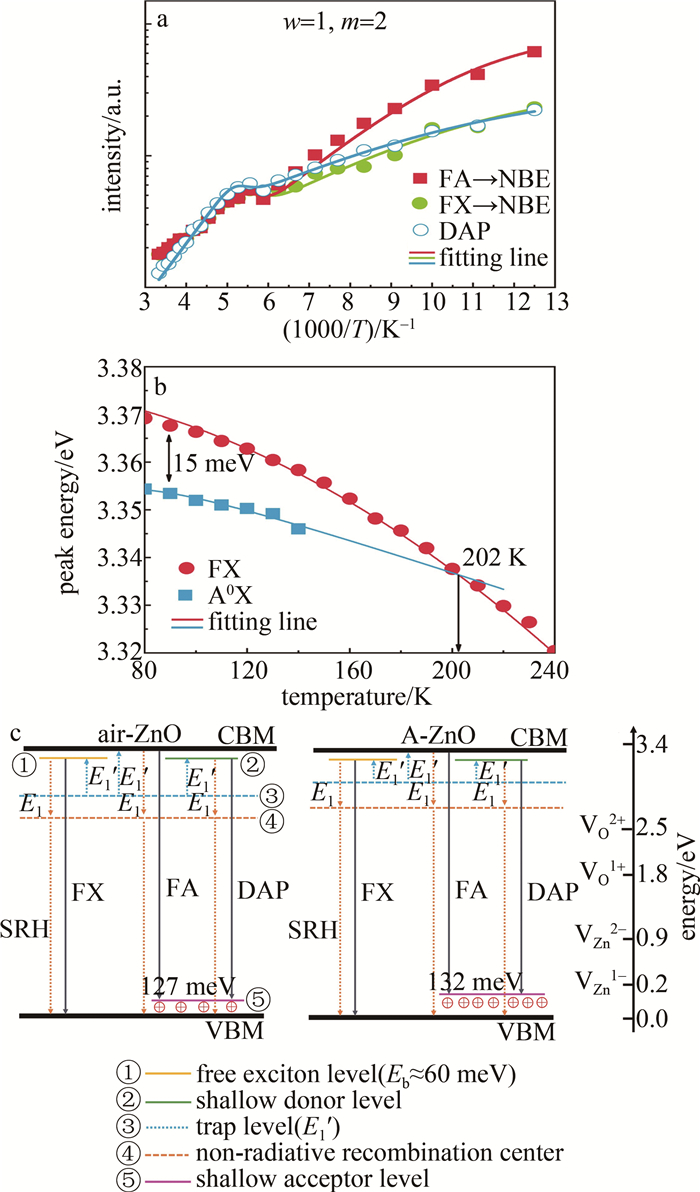
图 4 a—A-ZnO微米管的FA、FX和DAP发光峰强度随温度变化规律及其拟合曲线 b—A-ZnO微米管的FX和A0X发光峰能量随温度变化规律及其拟合曲线 c—air-ZnO微米管和A-ZnO微米管能带结构示意图
Figure 4. a—intensities of FA, FX and DAP emission of A-ZnO with temperature, and the corresponding fitting curves b—photon energies of FX and A0X emission of A-ZnO with temperature, and the corresponding fitting curves c—energy level diagrams of air-ZnO microtube and A-ZnO microtube, respectively
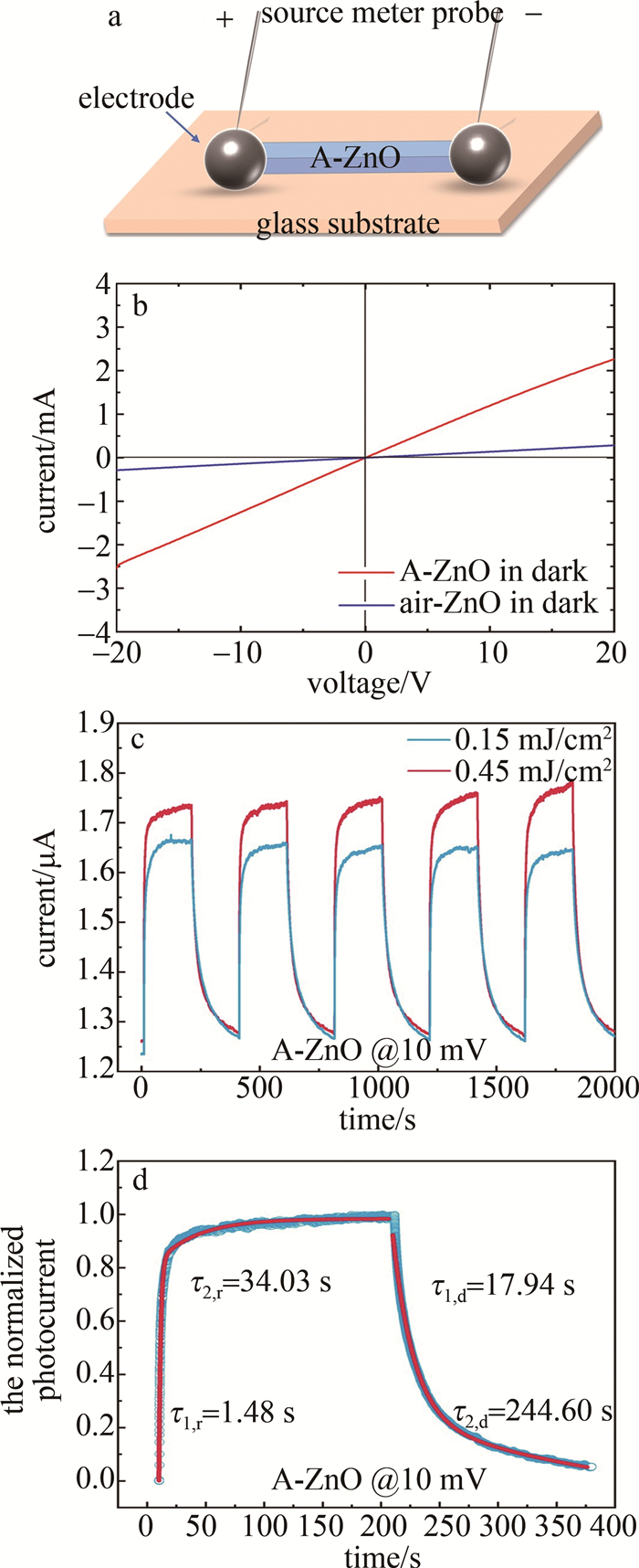
图 5 a—A-ZnO微米管光电探测器结构示意图 b—A-ZnO微米管与air-ZnO微米管电流对应电压的变化曲线 c—不同光能量密度下A-ZnO微米管的光电流响应特性 d—A-ZnO微米管归一化的光电流响应特性
Figure 5. a—schematic of the A-ZnO microtube detector b—voltage corresponding to current of A-ZnO microtubes and air-ZnO microtubes c—photocurrent response of A-ZnO microtube under various light energy intensity d—the normalized photocurrent response of A-ZnO microtube
-
[1] 申德振, 梅增霞, 梁会力, 等. 氧化锌基材料、异质结构及光电器件[J]. 发光学报, 2014, 35(1): 1-60. SHEN D Zh, MEI Z X, LIANG H L, et al. ZnO-based material, heterojunction and photoelctronic device[J]. Chinese Journal of Luminescence, 2014, 35(1): 1-60(in Chinese).
[2] 黄丰, 郑伟, 王梦晔, 等. 氧化锌单晶生长、载流子调控与应用研究进展[J]. 人工晶体学报, 2021, 50(2): 209-243. HUANG F, ZHENG W, WANG M Y, et al. Development of zinc oxide: Bulk crystal growth, arbitrary regulation of carrier concentration and practical applications[J]. Journal of Synthetic Crystals, 2021, 50(2): 209-243(in Chinese).
[3] 谢修为, 李炳辉, 张振中, 等. 点缺陷调控: 宽禁带Ⅱ族氧化物半导体的机遇与挑战[J]. 物理学报, 2019, 68(16): 167802. XIE X W, LI B H, ZHANG Zh Zh, et al. Point defects: Key issues for Ⅱ-oxides wide-bandgap semiconductors development[J]. ActaPhysicasinica, 2019, 68(16): 167802(in Chinese).
[4] JANOTTI A, van de WALLE C G. Native point defects in ZnO[J]. Physical Review, 2007, B76(16): 165202.
[5] KURBANOV S S, PANIN G N, KANG T W. Spatially resolved investigations of the emission around 3.31 eV (A-line) from ZnO nanocrystals[J]. Applied Physics Letters, 2009, 95(21): 211902. DOI: 10.1063/1.3264084
[6] SUSHAMA S, MURKUTE P, GHADI H, et al. Enhancement in structural, elemental and optical properties of boron-phosphorus Co-doped ZnO thin films by high-temperature annealing[J]. Journal of Luminescence, 2021, 238: 118221. DOI: 10.1016/j.jlumin.2021.118221
[7] SHIRRA M, SCHNEIDER R, REISER A, et al. Stacking fault related 3.31 eV luminescence at 130 meV acceptors in zinc oxide[J]. Physical Review, 2008, B77(12): 125215.
[8] WANG Q, YAN Y Zh, ZENG Y, et al. Free-standing undoped ZnO microtubes with rich and stable shallow acceptors[J]. Scientific Reports, 2016, 6: 27341.
[9] WANG Q, YAN Y Zh, ZENG Y, et al. Experimental and numerical study on growth of high-quality ZnO single-crystal microtubes by optical vapor supersaturated precipitation method[J]. Journal of Crystal Growth, 2017, 468: 638-644.
[10] WANG Q, YAN Y Zh, QIN F F, et al. A novel ultra-thin-walled ZnO microtube cavity supporting multiple optical modes for bluish-violet photoluminescence, low-threshold ultraviolet lasing and micro-fluidic photodegradation[J]. NPG Asia Materials, 2017, 9: e442.
[11] XING C, LIU W, WANG Q, et al. Current-induced thermal tunneling electroluminescence in a single highly compensated semiconductor microrod[J]. Iscience, 2020, 23(6): 101210.
[12] PAN Y M, YAN Y Zh, WANG Q, et al. Efficient defect control of zinc vacancy in undoped ZnO microtubes for optoelectronic applications[J]. Journal of Applied Physics, 2022, 131(10): 105105.
[13] 秦莉, 张喜田, 梁瑶, 等. 氧化锌微米花的共振拉曼和"负热淬灭"效应[J]. 物理学报, 2006, 55(6): 3120-3121. QIN L, ZHANG X T, LIANG Y, et al. Resonant Raman scattering and "negative thermal quenching" of ZnO microflowers[J]. Acta Physica Sinica, 2006, 55(6): 3120-3121(in Chinese).
[14] 王强, 杨立学, 刘北云, 等. 本征富受主型ZnO微米管光致发光的温度调控机制[J]. 物理学报, 2020, 69(19): 197701. WANG Q, YANG L X, LIU B Y, et al. Thermal regulation mechanism of photoluminescence in intrinsic acceptor-rich ZnO microtube[J]. Acta Physica Sinica, 2020, 69(19): 197701(in Chinese).
[15] CUSCO R, ALARCON-LLADO E, IBANEZ J, et al. Temperature dependence of Raman scattering in ZnO[J]. Physical Review, 2007, B75(16): 165202.
[16] SIMA M, MIHUT L, VASILE E, et al. Optical properties of Mn doped ZnO films and wires synthesized by thermal oxidation of ZnMn alloy[J]. Thin Solid Films, 2015, 590: 141-147.
[17] ZHAO J, YAN X Q, YANG Y, et al. Raman spectra and photoluminescence properties of In-doped ZnO nanostructures[J]. Materials Letters, 2010, 64(5): 569-572.
[18] TAY Y Y, SUN C Q, CHEN P. Size dependence of Zn 2p 3/2 binding energy in nanocrystalline ZnO[J]. Applied Physics Letters, 2006, 88(17): 173118.
[19] CHEN M, WANG X, YU Y H, et al. X-ray photoelectron spectroscopy and auger electron spectroscopy studies of Al-doped ZnO films[J]. Applied Surface Science, 2000, 158(1-2): 134-140.
[20] 侯清玉, 郭少强, 赵春旺. 氧空位浓度对ZnO电子结构和吸收光谱影响的研究[J]. 物理学报, 2014, 63(14): 147101. HOU Q Y, G Sh Q, ZHAO Ch W. First-principle study of the effects of oxygen vacancy on the electronic structure and the absorption spectrum of ZnO[J]. Acta Physica Sinica, 2014, 63(14): 147101(in Chinese).
[21] TU N, VAN BUI H, TRUNG D Q, et al. Surface oxygen vacancies of ZnO: A facile fabrication method and their contribution to the photoluminescence[J]. Journal of Alloys and Compounds, 2019, 791: 722-729.
[22] PRZEZDZIECKA E, KAMINSKA E, PASTERNAK I, et al. Photoluminescence study of p-type ZnO∶Sb prepared by thermal oxidation of the Zn-Sb starting[J]. Physical Review, 2007, B76(19): 193303.
[23] 赵涛, 李清山, 董艳锋, 等. 氧压对PLD制备掺铜ZnO薄膜光学性质的影响[J]. 激光技术, 2011, 35(6): 781-783. DOI: 10.3969/j.issn.1001-3806.2011.06.016 ZHAO T, LI Q Sh, DONG Y F, et al. Effect of oxygen pressure on optical properties of Cu-doped ZnO thin films prepared by PLD[J]. Laser Technology, 2011, 35(6): 781-783(in Chinese). DOI: 10.3969/j.issn.1001-3806.2011.06.016
[24] 霍艳丽, 李少兰, 马自侠. 溶液浓度对ZnO纳米棒形貌和发光的影响[J]. 激光技术, 2012, 36(6): 776-779. DOI: 10.3969/j.issn.1001-3806.2012.06.016 HU Y L, LI Sh L, MA Z X. Effect of solution concentration on the morphology and photoluminescence of ZnO nanorods[J]. Laser Technology, 2012, 36(6): 776-779(in Chinese). DOI: 10.3969/j.issn.1001-3806.2012.06.016
[25] CONRADT J, SARTOR J, THIELE C, et al. Catalyst-free growth of zinc oxide nanorod arrays on sputtered aluminum-doped zinc oxide for photovoltaic applications[J]. Journal of Physical Chemistry, 2011, C115(9): 3539-3543.
[26] TEKE A, OZGUR U, DOGAN X, et al. Excitonic fine structure and recombination dynamics in single-crystalline ZnO[J]. Physical Review, 2004, B70(19): 195207.
[27] HU L N, WANG Y, JIANG Y J, et al. N-ion-implanted ZnO microtubes for highly-efficient UV detection[J]. Optical Materials, 2023, 138: 113683.
[28] LOOK D C, REYNOLDS D C, LITTON C W, et al. Characterization of homoepitaxialp-type ZnO grown by molecular beam epitaxy[J]. Applied Physics Letters, 2002, 81(10): 1830-1832.
[29] ODONNELL K P, CHEN X. Temperature-dependence of semiconductor band-gaps[J]. Applied Physics Letters, 1991, 58(25): 2924-2926.
[30] SHIBATA H. Negative thermal quenching curves in photoluminescence of solids[J]. Japanese Journal of Applied Physics, 1998, 37(2): 550-553.
[31] 廖逸民, 闫胤洲, 王强, 等. ZnO微米晶的激光制备及发光性能研究[J]. 光谱学与光谱分析, 2022, 42(10): 3001-3005. LIAO Y M, YAN Y Zh, WANG Q, et al. Laser-induced growth device and optical properties of ZnO microcrystals[J]. Spectroscopy and Spectral Analysis, 2022, 42(10): 3001-3005(in Chinese).
[32] VARSHNI Y P. Temperature dependence of the energy gap in semiconductors[J]. Physica, 1967, 34(1): 149-154.
[33] HUANG Z H, YAN Y Zh, XING Ch, et al. Enhanced properties of hierarchically-nanostructured undoped acceptor-rich ZnO single-crystal microtube irradiated by UV laser[J]. Journal of Alloys and Compounds, 2019, 789: 841-851.
[34] 齐俊杰, 徐旻轩, 胡小峰, 等. 一维纳米氧化锌自驱动紫外探测器的构建与性能研究[J]. 物理学报, 2015, 64(17): 172901. QI J J, XU M X, HU X F, et al. Frabrication and properties of self-powered ultraviolet detectors based on one-demensional ZnO nanomaterials[J]. Acta Physica Sinica, 2015, 64(17): 172901(in Chinese).
[35] 郭亮, 赵东旭, 张振中, 等. 退火处理对ZnO纳米线紫外探测器性能的改善[J]. 发光学报, 2011, 32(8): 844-847. GUO L, ZHAO D X, ZHANG Zh Zh, et al. Effects of annealing treatmenton on ZnO nonowires used for utraviotet detector[J]. Chinese Journal of Luminescence, 2011, 32(8): 844-847(in Chinese).
[36] ZENG Y J, YE Z Z, LU Y F, et al. Investigation on ultraviolet photoconductivity in p-type ZnO thin films[J]. Chemical Physics Letters, 2007, 441(1/3): 115-118.
[37] ZHENG Zh Y, LIU K W, CHEN X, et al. High-performance flexible UV photodetector based on self-supporting ZnO nano-networks fabricated by substrate-free chemical vapor deposition[J]. Nanotechnology, 2021, 32(48): 475201.
[38] LI G D, ZHANG H, MENG L X, et al. Adjustment of oxygen vacancy states in ZnO and its application in ppb-level NO2 gas sensor[J]. Science Bulletin, 2020, 65(19): 1650-1658.


 下载:
下载:


