128-channel OPA based on SiN slab waveguide grating antenna
-
摘要: 为了避免全硅光学相控阵(OPA)的输出光功率饱和现象以及氮化硅的低移相效率,采用硅与氮化硅相结合的设计思路, 在实现高功率输入的同时保证了调相效率;此外,硅基集成OPA为了避免通道间的相互耦合所引起的相位噪声,波导间距大于半波长,导致栅瓣的存在,进而使得扫描范围受限,故采用硅波导作为天线前的输入波导, 以减小阵元间距。结果表明,芯片最终实现了41°×7.4°的扫描范围以及10.7 dB的芯片损耗。该研究对于OPA芯片的进一步改进是有帮助的。Abstract: In order to avoid the saturation phenomenon of output optical power of all silicon optical phased array (OPA) and the low phase shifting efficiency of silicon nitride, a design concept combining silicon and silicon nitride was adopted, which ensured the phase shifting efficiency while achieving high power input. In addition, in order to avoid phase noise caused by mutual coupling between channels, silicon-based integrated OPA had waveguide spacing greater than half wavelength, which led to the presence of gate lobes and limited the scanning range. To solve this problem, a silicon waveguide was used as the input waveguide in front of the antenna to reduce the array elements spacing. The results show that, the chip ultimately achieves a scanning range of 41°×7.4° and a chip loss of 10.7 dB. This study is helpful for further improvement of OPA chips.
-
Keywords:
- integrated optics /
- diffraction /
- gratings /
- optical phased array
-
-
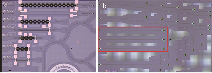
图 5 a—基于Si热光移相器的马赫-曾德尔调制器特性 b—级联SiN多模干涉耦合器各端口输出功率 c—Si和SiN波导模斑转换器的损耗
Figure 5. a—characterization of Mach-Zehnder modulator based on the silicon thermo-optic phase shifter b—output power at each port of the cascaded silicon nitride multimode interferometric coupler c—losses of silicon and silicon nitride waveguide spot size converters
-
[1] POULTON C V, BYRD M J, RUSSO P, et al. Long-range LiDAR and free-space data communication with high-performance optical phased arrays[J]. IEEE Journal of Selected Topics in Quantum Electronics, 2019, 25(5): 1-8.
[2] BHARGAVA P, KIM T, POULTON C V, et al. Fully integrated coherent LiDAR in 3D-integrated silicon photonics/65 nm CMOS[C]//2019 Symposium on VLSI Circuits. New York, USA: IEEE Press, 2019: C262-C263.
[3] BABA T, TAMANUKI T, ITO H, et al. Silicon photonics FMCW LiDAR chip with a slow-light grating beam scanner[J]. IEEE Journal of Selected Topics in Quantum Electronics, 2022, 28(5): 1-8.
[4] ABIRI B, FATEMI R, HAJIMIRI A. A 1-D heterodyne lens-free optical phased array camera with reference phase shifting[J]. IEEE Photonics Journal, 2018, 10(5): 1-12.
[5] BYRD M J, POULTON C V, KHANDAKER M, et al. Free-space communication links with transmitting and receiving integrated optical phased arrays[C]//Frontiers in Optics/Laser Science. New York, USA: IEEE Press, 2018: FTu4E. 1.
[6] CLEVENSON H A, SPECTOR S J, BENNEY L, et al. Incoherent light imaging using an optical phased array[J]. Applied Physics Le-tters, 2020, 116(3): 031105. DOI: 10.1063/1.5130697
[7] BHANDARI B, WANG ChX, GWON J Y, et al. Integrated optical phased array enabling wavelength-tuned line scanning[C]//2022 27th Opto-Electronics and Communications Conference (OECC) and 2022 International Conference on Photonics in Switching and Computing (PSC). New York, USA: IEEE Press, 2022: 1-3.
[8] KIM J Y, YOON J, KIM J, et al. Demonstration of beam steering using a passive silica optical phased array with wavelength tuning[J]. Optics Letters, 2022, 47(19): 4857-4860. DOI: 10.1364/OL.470667
[9] YU L, WANG P, MA P, et al. Two-dimensional beam scanning of passive optical phased array based on silicon nitride delay line[J]. Journal of Lightwave Technology, 2023, 41(9): 2756-2764.
[10] MISUGI Y, OKAYAMA H, KITA T. Demonstration of 2D beam steering using large-scale passive optical phased array enabled by multimode waveguides with reduced phase error[J]. Applied Phy-sics Express, 2022, 15(10): 102002. DOI: 10.35848/1882-0786/ac9033
[11] MISUGI Y, OKAYAMA H, KITA T. Compact and low power-consumption solid-state two-dimensional beam scanner integrating a pa-ssive optical phased array and hybrid wavelength-tunable laser diode[J]. Journal of Lightwave Technology, 2023, 41(11): 3505-3512. DOI: 10.1109/JLT.2023.3244847
[12] POULTON C V, BYRD M J, RAVAL M, et al. Large-scale silicon nitride nanophotonic phased arrays at infrared and visible wavelengths[J]. Optics Letters, 2017, 42(1): 21-24. DOI: 10.1364/OL.42.000021
[13] IM C S, BHANDARI B, LEE K P, et al. Silicon nitride optical phased array based on a grating antenna enabling wavelength-tuned beam steering[J]. Optics Express, 2020, 28(3): 3270-3279. DOI: 10.1364/OE.383304
[14] LI Y, CHEN B, NA Q, et al. Wide-steering-angle high-resolution optical phased array[J]. Photonics Research, 2021, 9(12): 2511-2518. DOI: 10.1364/PRJ.437846
[15] WANG Q, WANG S, JIA L, et al. Silicon nitride assisted 1×64 optical phased array based on a SOI platform[J]. Optics Express, 2021, 29(7): 10509-10517. DOI: 10.1364/OE.420921
[16] LUO G, YU L, MA P, et al. A large-scale passive optical phase array with 1024 channels[J]. IEEE Photonics Technology Letters, 2023, 35(17): 927-930. DOI: 10.1109/LPT.2023.3289231
[17] WANG P F, LUO G Zh, XU H Y, et al. Design and fabrication of a SiN-Si dual-layer optical phased array chip[J]. Photonics Research, 2020, 8(6): 06000912.
[18] LUO G, WANG P, MA J, et al. Demonstration of 128-channel optical phased array with large scanning range[J]. IEEE Photonics Journal, 2021, 13(3): 1-10.
[19] LIU Y, HU H. Silicon optical phased array with a 180-degree field of view for 2D optical beam steering[J]. Optica, 2022, 9(8): 903-907. DOI: 10.1364/OPTICA.458642
[20] TYLER N A, FOWLER D, MALHOUITRE S, et al. SiN integrated optical phased arrays for two-dimensional beam steering at a single near-infrared wavelength[J]. Optics Express, 2019, 27(4): 5851-5858. DOI: 10.1364/OE.27.005851
[21] CHUL S M, MOHANTY A, WATSON K, et al. Chip-scale blue light phased array[J]. Optics Letters, 2020, 45(7): 1934-1937. DOI: 10.1364/OL.385201
[22] HSU C P, LI B, SOLANO-RIVAS B, et al. A review and perspective on optical phased array for automotive LiDAR[J]. IEEE Journal of Selected Topics in Quantum Electronics, 2021, 27(1): 1-16.
[23] SHANG K, QIN C, ZHANG Y, et al. Uniform emission, constant wavevector silicon grating surface emitter for beam steering with ultra-sharp instantaneous field-of-view[J]. Optics Express, 2017, 25(17): 19655. DOI: 10.1364/OE.25.019655
[24] RAVAL M, POULTON C V, WATTS M R. Unidirectional waveguide grating antennas with uniform emission for optical phased arrays[J]. Optics Letters, 2017, 42(13): 2563-2566. DOI: 10.1364/OL.42.002563
[25] YU L, MA P, LUO G, et al. Adoption of large aperture chirped grating antennas in optical phase array for long distance ranging[J]. Optics Express, 2022, 30(15): 28112-28120. DOI: 10.1364/OE.464358
[26] ZHANG L, WANG Y, HOU Y, et al. Uniform rectangular distribution of far-field intensity by optical phased array[J]. Optics Communications, 2022, 507: 127661. DOI: 10.1016/j.optcom.2021.127661
[27] KOMLJENOVIC T, HELKEY R, COLDREN L, et al. Sparse aperiodic arrays for optical beam forming and LiDAR[J]. Optics Express, 2017, 25(3): 2511-2528. DOI: 10.1364/OE.25.002511
[28] FATEMI R, KHACHATURIAN A, HAJIMIRI A. A nonuniform sparse 2-D large-FOV optical phased array with a low-power PWM drive[J]. IEEE Journal of Solid-State Circuits, 2019, 54(5): 1200-1215. DOI: 10.1109/JSSC.2019.2896767
[29] POLKOO S S, RENSHAW C K. Hybrid imaging-based beam steering system using a sparse photonic integrated circuit outcoupling array[C]//Conference on Lasers and Electro-Optics. New York, USA: IEEE Press, 2020: JTh2B. 25.
[30] POULTON C V, BYRD M J, RUSSO P, et al. Coherent LiDAR with an 8, 192-element optical phased array and driving laser[J]. IEEE Journal of Selected Topics in Quantum Electronics, 2022, 28(5): 6100508.
[31] SAYYAH K, SARKISSIAN R, PATTERSON P, et al. Fully integrated FMCW LiDAR optical engine on a single silicon chip[J]. Journal of Lightwave Technology, 2022, 40(9): 2763-2772. DOI: 10.1109/JLT.2022.3145711
[32] WANG P F, LUO G Z, YU H Y, et al. Improving the performance of optical antenna for optical phased arrays through high-contrast grating structure on SOI substrate[J]. Optics Express, 2019, 27(3): 2703-2712. DOI: 10.1364/OE.27.002703
[33] HAN K, YURLOV V, YU N E. Highly directional waveguide grating antenna for optical phased array[J]. Current Applied Physics, 2018, 18(7): 824-828. DOI: 10.1016/j.cap.2018.04.004
[34] 郑伟, 王超, 杨文丽, 等. 基于色散光学的光波束形成网络[J]. 激光技术, 2022, 46(2): 188-192. DOI: 10.7510/jgjs.issn.1001-3806.2022.02.007 ZHENG W, WANG Ch, YANG W L, et al. An optical beamforming network based on dispersing optics[J]. Laser Technology, 2022, 46(2): 188-192(in Chinese). DOI: 10.7510/jgjs.issn.1001-3806.2022.02.007


 下载:
下载:
