Research of effect of guide-mode resonance grating parameters on resonance wavelength and line width
-
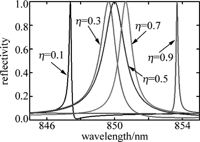
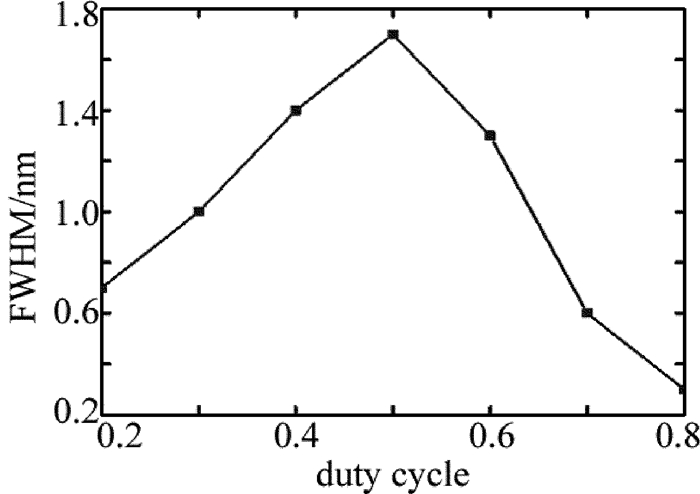
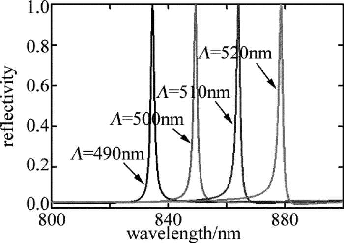
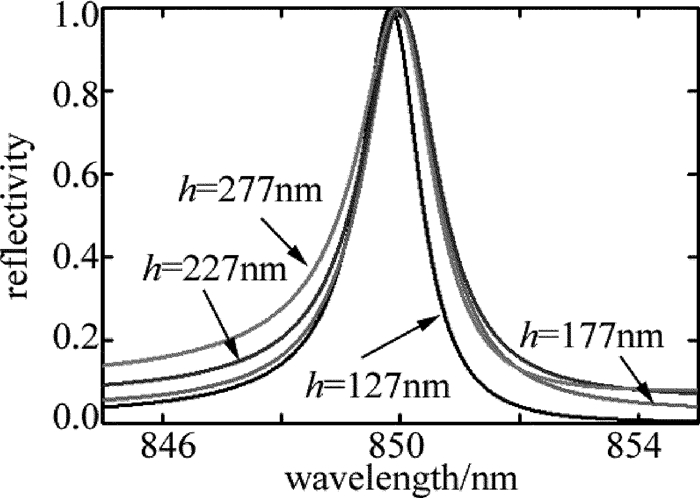
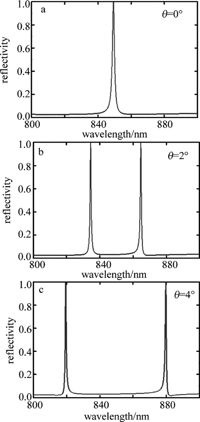
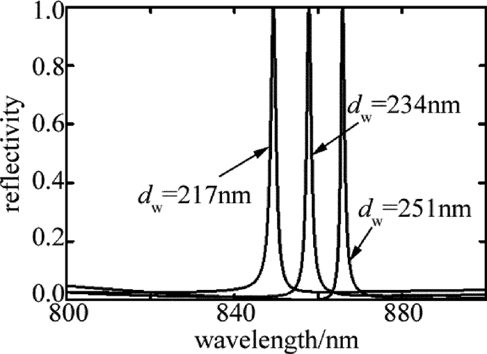
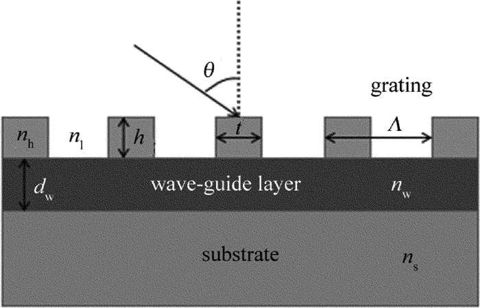
摘要: 为了能够设计出具有反射功能的导模共振光栅,采用光栅的等效介质理论、平面波导理论以及严格耦合波法,进行了理论分析和实验验证,设计了在TE偏振下波长850nm处具有反射共振的导模共振光栅。利用严格耦合波法,计算并分析了光栅参量、入射角以及波导层厚度对共振波长和线宽的影响。结果表明,随着占空比的增大,共振波长会红移,而共振线宽会随着占空比的增大先增后减,占空比为0.5时线宽能达到最宽;共振波长会随着光栅周期和波导层厚度的增大而增大,但线宽几乎不变,当周期从490nm增加到520nm时,共振波长红移了将近50nm,而当波导层厚度从217nm增加到251nm时,共振波长红移了将近25nm;光栅厚度变化对共振波长和共振线宽影响很微弱,当入射角是垂直入射时仅有一个共振峰,但是当入射角不为0°时会出现两个共振峰,并且两个共振波长随着入射角度的变大一个会蓝移而另一个则红移。该研究为实际制备反射导模共振光栅提供了理论指导。Abstract: In order to design guided mode resonance gratings with reflection function, based on equivalent medium theory, planar waveguide theory and rigorous coupled wave analysis, theoretical analysis and experimental verification were carried out, guide-mode resonance gratings were designed to realize reflection resonance on 850nm (TE).The effects of grating parameters, incident angle and thickness of waveguide layer on resonance wavelength and linewidth were calculated by rigorous coupled wave method.The results show that, with the increase of duty cycle, resonance wavelength will shift red and resonance linewidth increases first and then decreases with the increase of duty cycle.When duty cycle is 0.5, line width can reach the widest.Resonant wavelength increases with the increase of grating period and waveguide layer thickness.But the line width is almost unchanged.When the period increases from 490nm to 520nm, resonance wavelength is red-shifted by nearly 50nm.When the thickness of waveguide layer increases from 217nm to 251nm, resonance wavelength is red-shifted by nearly 25nm.The influence of grating thickness on resonance wavelength and resonance linewidth is very weak.When the incident angle is perpendicular, there is only one resonance peak.But when the incident angle is not 0°, there will be two resonance peaks.And with the increase of incident angle, one resonance wavelength will be blue-shifted while the other will be red-shifted.This study provides theoretical guidance for practical preparation of reflective guided mode resonance gratings.
-
Keywords:
- gratings /
- resonance /
- rigorous coupled wave analysis /
- waveguide layer
-
-
-
[1] LI Sh, GUAN B L, SHI G Zh, et al. Polarization stable vertical-cavity surface-emitting laser with surface sub-wavelength gratings[J]. Acta Physica Sinica, 2012, 61(18):184208(in Chinese). http://d.old.wanfangdata.com.cn/Periodical/wlxb201218027
[2] LI X S, NING Y Q, ZHANG X, et al. Influence of grating parameters on reflectivity of Si/SiO2 high contrast gratings[J]. Chinese Journal of Luminescence, 2015, 36(7):806-810(in Chinese). DOI: 10.3788/fgxb
[3] HUANG M C Y, ZHOU Y, CHANGHASNAIN C J. A surface-emitting laser incorporating a high-index-contrast subwavelength grating[J].Nature Photonics, 2007, 297(1):119-122. http://cn.bing.com/academic/profile?id=aab3d19035422d7fd4e0234953aeefe6&encoded=0&v=paper_preview&mkt=zh-cn
[4] SONG M G, CAO L Q, LIU F M, et al. Optimized design of grating coupling packaging structure on silicon substrate[J]. Laser Technology, 2017, 41(4):479-483(in Chinese). http://www.jgjs.net.cn/EN/abstract/abstract15611.shtml
[5] ANSBAEK T, CHUNG I S, SEMENOVA E S, et al. 1060nm tunable monolithic high index contrast subwavelength grating VCSEL[J]. IEEE Photonics Technology Letters, 2013, 25(4):365-367. DOI: 10.1109/LPT.2012.2236087
[6] JIANG X W, GUAN B, LIU X, et al. The influence of sub-wavelength grating on wavelength tuning range in VCSEL[C]//2015 International Conference on Optoelectronics and Microelectronics. NewYork, USA: IEEE, 2016: 43-46.
[7] HAGLUND E, GUSTAVSSON J S, SORIN W V, et al. Multi-wavelength VCSEL arrays using high-contrast gratings[J]. Proceedings of the SPIE, 2017, 10113:101130B. DOI: 10.1117/12.2256348
[8] DAVANI H A, KOGEL B, DEBERNARDI P, et al. Polarization investigation of a tunable high-speed short-wavelength bulk-micromachined MEMS-VCSEL[J]. Proceedings of the SPIE, 2012, 8276:82760T. DOI: 10.1117/12.908262
[9] JIANG X W, GUAN B L. Polarization research of VCSEL based on sub-wavelength grating[J]. Chinese Journal of Luminescence, 2017, 38(6):729-734(in Chinese). DOI: 10.3788/fgxb
[10] HARRIS J S, SULLIVAN T O, SARMIENTO T, et al. Emerging applications for vertical cavity surface emitting lasers[J]. Semiconductor Science and Technology, 2011, 26(1):014010. DOI: 10.1088/0268-1242/26/1/014010
[11] TORRE M S, MASOLLER C. Fundamentals, technology and applications of vertical-cavity surface-emitting lasers[J].Berlin, Germary:Springer, 2014:120-122.
[12] DEGEN C, FISCHER I, ELSÄβER W. Transverse modes in oxide confined VCSELs:influence of pump profile, spatial hole burning, and thermal effects[J]. Optics Express, 1999, 5(3):38-47. DOI: 10.1364/OE.5.000038
[13] JAYARAMAN V, GOODNOUGH T J, BEAM T L, et al. Continuous-wave operation of single-transverse-mode 1310nm VCSELs up to 115/spl deg/C[J]. IEEE Photonics Technology Letters, 2000, 12(12):1595-1597. DOI: 10.1109/68.896318
[14] COX J A. Guided-mode grating resonant filters for VCSEL applications[J]. Proceedings of the SPIE, 1998, 3291:70-76. DOI: 10.1117/12.310571
[15] OLINER A A, HESSEL A. A new theory of Wood's anomalies on optical grating[J]. Applied Optics, 1965, 4(10):1275-1299. DOI: 10.1364/AO.4.001275
[16] WANG S S, MAGNUSSON R. Theory and application of guide-mode resonance folters[J]. Applied Optics, 1993, 32(14):2606-2613. DOI: 10.1364/AO.32.002606
[17] FU X, YI K, SHAO J, et al. Nonpolarizing guide-mode resonance filter[J]. Optics Letters, 2009, 34(2):122-124. http://d.old.wanfangdata.com.cn/Conference/WFHYXW463502
[18] BOYE R R, ZIOLKOWSKI R W, KOSTUK R K. Resonant waveguide mode-grating switching device with nonlinear optical material[J]. Applied Optics, 1999, 38(24):5181-5185. DOI: 10.1364/AO.38.005181
[19] SHARON A, GLASBERG S, ROSENBLATT D, et al. Metal-based resonant grating waveguide structures[J]. Journal of the Optical Society of America, 1997, A14(11):2038-2059. http://d.old.wanfangdata.com.cn/NSTLQK/NSTL_QKJJ028270761/
[20] CHARLES W H, LI L F. Effective-medium theory of zeroth-order lamellar gratings in conical mountings[J]. Journal of Optical Society of America, 1993, A10(10):2217-2225. DOI: 10.1364-JOSAA.10.002217/


 下载:
下载:
