Advanced Search

ISSN1001-3806 CN51-1125/TN Map

Volume 46 Issue 5
Sep.  2022
Article Contents
Turn off MathJax

Citation:

Influence of spontaneous radiation on detectors of different-shape radiation shields

  • Corresponding author: SONG Haizhi, hzsong1296@163.com
  • Received Date: 2021-08-10
    Accepted Date: 2021-09-02
  • In order to clarify the influence of the spontaneous radiation of different-shape shields on detectors and find out the shape that has the least impact, the spontaneous power to the detector from the inner shields with different shapes was systematically analyzed by theoretical calculation. The shapes of the shields include paraboloid, hyperboloid, semi-ellipsoid (including hemisphere), and frustum of cone (including cylinder and cone). The results showed that the spontaneous power to the detector of all shapes of shields first decreases and then increase with the increase of the ratio of the height of the shield to the radius of the bottom. The maximum radiation power is a constant related to the size of the detector, and the minima appear when the heights of the shields are close to or equal to the radiuses of the bottoms. When the shield is semi-ellipsoidal and the height is equal to the radius (i.e., hemisphere), the power of spontaneous radiation to the detector is less than that of any other shield, and it has nothing to do with the size of the shield or whether there are small holes on the top. This study can provide a valuable reference for the design of radiation shields.
  • 加载中
  • [1]

    ZHANG L B, KANG L, CHEN J, et al. Development of superconductor single-photon detector[J]. Electronic and Electro-optical Systems, 2010(4): 1-5(in Chinese).
    [2]

    YOU L X. Status and prospect of superconducting nanowire single photon detection[J]. Infrared and Laser Engineering, 2018, 47(12): 1202001(in Chinese). doi: 10.3788/IRLA201847.1202001
    [3]

    ALLMAN M S, VERMA V B, HORANSKY R, et al. Progress towards a near IR single-photon superconducting nanowire camera for free-space imaging of light[C]//CLEO: Applications and Technology. Piscataway, NJ, USA: IEEE, 2014: 1-2.
    [4]

    YAMASHITA T, LIU D, MIKI S, et al. Fluorescence correlation spectroscopy with visible-wavelength superconducting nanowire single-photon detector[J]. Optics Express, 2014, 22(23): 28783-28789. doi: 10.1364/OE.22.028783
    [5]

    LI H, CHEN S, YOU L, et al. Superconducting nanowire single photon detector at 532nm and demonstration in satellite laser ranging[J]. Optics Express, 2016, 24(4): 3535-3542. doi: 10.1364/OE.24.003535
    [6]

    EISAMAN M D, FAN J, MIGDALL A, et al. Invited review article: Single-photon sources and detectors[J]. Review of Scientific Instruments, 2011, 82(7): 071101. doi: 10.1063/1.3610677
    [7]

    NIWA K, NUMATA T, HATTORI K, et al. Few-photon color imaging using energy-dispersive superconducting transition-edge sensor spectrometry[J]. Scientific Reports, 2017, 7: 45660. doi: 10.1038/srep45660
    [8]

    SUN W, XIA Ch X, LI J, et al. Research on the influence of cold shield on the cooling process of infrared detector assembly[J]. Laser & Infrared, 2017, 47(10): 1286-1289(in Chinese).
    [9]

    LU J T, ZHANG X Y, LI Y H. Test and analysis of average BRDF in different blackening processes of cold shield[J]. Laser & Infrared, 2016, 46(2): 196-199(in Chinese).
    [10]

    LIU D K. Eletrical characteristics and large active-area research of superconducting nanowire single-photon detector[D]. Shanghai: University of Chinese Academy of Sciences, 2014: 34-36(in Chin-ese).
    [11]

    HU X L, XU L, ZOU K, et al. A superconductor nanowire single-photon detection system in the mid-infrared band: China, 201910888886.0[P]. 2020-01-17(in Chinese).
    [12]

    XIE X M, XU Q, CHEN J, et al. Research progress on antimonide based type Ⅱ superlattice mid- and long-infrared detectors[J]. Laser Technology, 2020, 44(6): 688-694(in Chinese).
    [13]

    SHI M L, LING L. Status and development trends of the HgCdTe large infrared focal array technology[J]. Journal of Ordnance Equipment Engineering, 2017, 37(11): 916-920(in Chinese).
    [14]

    GOPAL V, DHAR V. Cold radiation shield design for a linear detector array[J]. Infrared Physics, 1986, 26(2): 83-87. doi: 10.1016/0020-0891(86)90025-4
    [15]

    YE H F, YANG H M, WANG T J, et al. Anti-radiation screen assembly for cryogenic refrigerator: China, 201020155002.5[P]. 2010-11-24(in Chinese).
    [16]

    YIN Sh, ZHU Y F, HUANG Y B, et al. The stray radiation su-ppression of the baffles of infrared focal plane dewar[J]. Infrared Technology, 2015, 37(11): 916-920(in Chinese).
    [17]

    CHANG K, CHEN Sh Zh, WANG H, et al. Anti-radiation structure for low-temperature container: China, 201410172026[P]. 2016-03-30(in Chinese).
    [18]

    JIN N, YANG K Y, CAO L, et al. Optimization design for the shapes of cold shield in infrared systems[J]. Acta Optica Sinica, 2016, 36(1): 0111005(in Chinese). doi: 10.3788/AOS201636.0111005
    [19]

    WANG Zh L, LI P Y, ZHANG Y T, et al. Circulating cooling radiation shield: China, 201720307684.9[P]. 2017-10-20(in Chin-ese).
    [20]

    GONG J. Design method of large dimension cold shield based on G-M cryocooler[J]. Journal of Aerospace Power, 2019, 34(2): 341-347(in Chinese).
    [21]

    AI J, LI Z G, POPOV A K. Gas drift induced by laser-produced plasma radiation[J]. Laser Technology, 1992, 16(5): 257-261(in Chinese).
    [22]

    RANGANATH G S. Black-body radiation[J]. Resonance, 2008, 13(2): 115-133. doi: 10.1007/s12045-008-0028-7
  • 加载中
通讯作者: 陈斌, bchen63@163.com
  • 1. 

    沈阳化工大学材料科学与工程学院 沈阳 110142

  1. 本站搜索
  2. 百度学术搜索
  3. 万方数据库搜索
  4. CNKI搜索

Figures(5) / Tables(1)

Article views(5578) PDF downloads(26) Cited by()

Proportional views

Influence of spontaneous radiation on detectors of different-shape radiation shields

    Corresponding author: SONG Haizhi, hzsong1296@163.com
  • 1. Southwest Institute of Technical Physics, Chengdu 610041, China
  • 2. Institute of Fundamental and Frontier Sciences, University of Electronic Science and Technology of China, Chengdu 610054, China

Abstract: In order to clarify the influence of the spontaneous radiation of different-shape shields on detectors and find out the shape that has the least impact, the spontaneous power to the detector from the inner shields with different shapes was systematically analyzed by theoretical calculation. The shapes of the shields include paraboloid, hyperboloid, semi-ellipsoid (including hemisphere), and frustum of cone (including cylinder and cone). The results showed that the spontaneous power to the detector of all shapes of shields first decreases and then increase with the increase of the ratio of the height of the shield to the radius of the bottom. The maximum radiation power is a constant related to the size of the detector, and the minima appear when the heights of the shields are close to or equal to the radiuses of the bottoms. When the shield is semi-ellipsoidal and the height is equal to the radius (i.e., hemisphere), the power of spontaneous radiation to the detector is less than that of any other shield, and it has nothing to do with the size of the shield or whether there are small holes on the top. This study can provide a valuable reference for the design of radiation shields.

引言
  • 防辐射屏在自由空间激光探测,特别是在以超导单光子探测器为代表的低温弱光探测领域起着重要的作用。超导单光子探测器具有暗计数率低、灵敏度高、响应速度快等特点,在极弱光激光3维成像、光谱学、量子通信、预警、制导等领域具有广阔的应用前景[1-7]。由于超导单光子探测器工作温度极低(通常10K以下),与环境温度相差极大,因此为了减小环境对探测器制冷效果的影响[8],同时抑制环境背景辐射,提高信噪比,需要在探测器性能测试及组件应用时在探测器外设置防辐射屏(冷屏)[9]。由于常规超导探测器只能响应近红外以下波段,故通常采用小型屏蔽罩将引入光信号的光纤封装在防辐射屏内部[10],对高性能防辐射屏的需求不是很强烈。但随着新型超导单光子探测器响应波长向中远红外扩展[11],又没有成熟的能够在极低温下工作的中远红外光纤,超导探测器测试及应用时需要直接暴露在防辐射屏下。目前直接暴露在防辐射屏下的应用主要是工作温度相对较高且灵敏度相对较低的InAs/GaSb Ⅱ类超晶格[12]、碲镉汞[13]等中远红外探测器,其对防辐射屏的自发辐射不敏感,因此多直接采用圆柱形或台柱形结构。

    1986年,GOPAL等人[14]通过计算分析了防辐射屏上不同长宽比的矩形开孔对线列探测器的视场遮挡和外界辐射抑制效果,并给出了抑制外界辐射的同时提高探测器均匀性的防辐射屏开口设计折中方案。2010年,YE等人[15]通过在低温容器内增加防辐射屏组件,有效减小了低温容器内外的热传导,降低了内部温度。2015年,YIN等人[16]采用光学设计软件,分析了不同开孔形状的冷屏对杂散光的抑制效果,给出了开孔形状设计优化方案。2016年,LU等人[9]研究了冷屏表面不同工艺制备的黑化涂层的中远红外反射谱,为不同谱段工作的低温探测器冷屏表面设计提供了参考。同年,CHANG等人[17]设计了柱状同轴双层防辐射屏结构,有效减小了外界环境对内部低温背景的影响。同年,JIN等人[18]通过建立优化变量和优化目标函数的数学模型,采用区间穷举法和阻尼最小二乘法优化了防辐射屏开孔形状,极大抑制了杂散光对低温器件的影响。2017年,WANG等人[19]发明了一种循环冷却的防辐射屏,通过氦气管对防辐射屏表面进行持续冷却,确保防辐射屏保持超低温,减小了对元器件的自发辐射。2019年,GONG[20]提出了基于Gifford-Mcmahon(G-M)制冷机的防辐射屏设计方法,通过冷缩补偿、表面温度分布及降温时间计算分析等手段,成功研制了能够为红外定标试验提供高均匀的低温冷背景的大尺寸防辐射屏。

    由此可见,前期研究人员对防辐射屏的研究重点主要集中在抑制外界杂散光及开孔形状优化[14, 16, 18]、减小内外热传导[15, 17]、降低防辐射屏温度[19]、增加温度均匀性[20]、优化低反射系数和低发射率涂层材料及工艺[9]等方面,而对防辐射屏的形状影响鲜有研究。防辐射屏的温度(例如70K)相对超导探测器来说仍然较高,且探测器为中远红外单光子响应,因此,防辐射屏形状变化引起的自发辐射也会对探测器的性能造成很大影响。

    针对极低温度下超导单光子探测器,特别是中远红外单光子探测器的测试及应用对自发辐射极低的防辐射屏需求,本文中系统研究了在一定物理空间内,形状为抛物面、双曲面、半椭球面(含半球面)、台柱面(含圆柱面和圆椎面)的防辐射屏内屏自发辐射对探测器的影响,给出了自发辐射至探测器最小的防辐射屏形状,能够为防辐射屏结构设计提供有价值的参考。

1.   防辐射屏结构模型
  • 不同形状防辐射屏如图 1所示。其中小图为各形状内屏的3维结构示意图。为简化作图,抛物面、双曲面和半椭球面内屏纵向截面均采用图 1a进行示意。为消除横向尺度不同的影响,探测器所在冷头平面与防辐射屏交界面为半径为R的圆形,且探测器位于圆形中心,其有效半径为r,尺寸(微米至数十微米量级)远小于防辐射屏(厘米至数十厘米量级)。所有防辐射屏高度均为D。对于半椭球面防辐射屏,探测器位于椭球中心;当D=R时,半椭球面辐射屏变为半球面辐射屏。对于台柱面防辐射屏,其顶部半径为R′,当R′=0时,台柱面变为圆椎面;当R′=R时,台柱面变为圆柱面。防辐射屏上任意一点到探测器中心的距离为d,任一点和探测器中心连线与探测器法线的夹角为θ

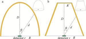
    Figure 1.  Schematic diagrams of different shapes of radiation shields(the insets illustrating the 3-D structures)

  • 根据黑体辐射定律[21-22],防辐射屏单位面积的自发辐射功率(辐射出射度)为:

    式中,λ1λ2为积分计算的上下截止波长,可根据实际情况选取不同的波段;h为普朗克常数;c为真空中的光速;η(λ)为材料在λ波长的发射率,与防辐射屏材料表面性质(涂层)和相应的发射波长有关;k为玻尔兹曼常数;T为防辐射屏温度。可见辐射出射度M只与防辐射屏温度和材料表面性质有关。

    由于本文中只关注防辐射屏形状的影响,因此,设定所有防辐射屏内屏表面材料相同,温度相等且均匀分布。同时为了简化讨论并结合实际情况,设定防辐射屏内屏表面涂层的反射系数极小,故不考虑自发辐射经防辐射屏反射至探测器的情况。

  • 抛物面上任一点到探测器中心的距离为:

    抛物面防辐射屏自发辐射至探测器的功率,可视为防辐射屏上垂直于探测器法线的圆形微环自发辐射至探测器功率的积分。由于防辐射屏上每个垂直于探测器法线的圆形微环上的所有微元辐射至探测器的功率相等,且rd,因此,每个微环辐射至探测器的功率可视为半径为d的球面波在探测器法线方向的分量:

    式中,Sr为探测器面积,Sd为半径为d的半球面积,dS=2πdsinθdL为微环面积,dL为微环宽度:

    其中,

    故抛物面防辐射屏自发辐射至探测器的总功率为:

  • 双曲面(一支)上任一点到探测器中心的距离为:

    式中,a>0和$b=a R / \sqrt{D^2+2 a D} $为双曲面在计算坐标系中的相对位置参数。

    与抛物面类似,双曲面防辐射屏自发辐射至探测器的功率,可视为防辐射屏上垂直于探测器法线的圆形微环自发辐射至探测器功率的积分。微环宽度为:

    式中,

    故一支双曲面防辐射屏辐射至探测器的功率为:

    式中,虽然仍有双曲面在坐标系中的相对位置参数ab,但实际上数值积分后双曲面防辐射屏自发辐射至探测器的功率与其无关。

  • 半椭球面上任一点到探测器中心的距离为:

    与抛物面类似,半椭球面防辐射屏自发辐射至探测器的功率,可视为防辐射屏上垂直于探测器法线的圆形微环自发辐射至探测器功率的积分。微环宽度为:

    故整个半椭球面防辐射屏辐射至探测器的功率为:

    D=R时,半椭球面变为半球面,其辐射至探测器的功率为:

    即半球面防辐射屏自发辐射至探测器的功率与防辐射屏尺寸无关,只与内屏温度和表面材料性质有关。

  • 常规台柱面防辐射屏结构如图 1b所示,分为顶部和侧壁两部分。对于顶部,其自发辐射至探测器的有效功率容易得到:

    对于侧壁的自发辐射,采用与前面同样的处理方法,即侧壁圆形微环辐射功率积分。侧壁上任意一点到探测器的距离为:

    侧壁微环宽度为:

    故台柱面防辐射屏自发辐射至探测器的总的有效功率为:

    R′=0时,台柱面变为圆椎面,其辐射至探测器的功率为:

    R′=R时,台柱面变为圆柱面,其辐射至探测器的功率为:

2.   结果分析
  • 不同形状的防辐射屏自发辐射至探测器的功率如图 2所示。其中台柱面防辐射屏给出了R′/R=0(圆椎面)、R′/R=1(圆柱面)和R′/R=0.5(普通台柱面)进行示意。可以看到,所有形状的防辐射屏底面半径R相同时,其自发辐射至探测器的功率均随防辐射屏高度的增加而先减小后增大,且最大值趋于常数πr2M,即最大值只与探测器尺寸有关;最小值出现在防辐射屏高度与底面半径接近(抛物面、双曲面、普通台柱面)或相等(半椭球面、圆柱面、圆椎面)时,其中椭球面、圆柱面、圆椎面自发辐射的最小值有解析式。半椭球面防辐射屏自发辐射至探测器的最小值(此时半椭球面即为半球面)见(17) 式。

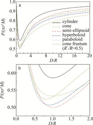
    Figure 2.  Spontaneous radiation power of different-shape shields to the detector

    圆柱面防辐射屏自发辐射至探测器的最小值为:

    圆椎面防辐射屏自发辐射至探测器的最小值为:

    在相同的D/R下,圆柱面防辐射屏辐射至探测器的功率比其它形状防辐射屏的都大,其它形状防辐射屏的辐射功率大小则互有交叉。抛物面和双曲面防辐射屏辐射至探测器的功率在D/R较小时几乎相等,但随着D/R的增大,双曲面表现出更小的辐射功率。

    对于普通台柱面防辐射屏,底面半径R相同时,其最小辐射功率随顶部半径R′的变化而不同。不同R′/R的台柱形防辐射屏的最小辐射功率如图 3所示,图中也示出了其它几种形状防辐射屏的辐射最小值进行直观对比。可见台柱面防辐射屏底面半径不变时,其对探测器的自发辐射功率最小值随着顶部半径的增大(即台柱面逐渐从圆椎面逐渐变为圆柱面)先减小后增大,但自发辐射最小值(位于R′/R=0.38处)仍然比球面防辐射屏的最小值大,也大于椭球面和双曲面的辐射最小值。

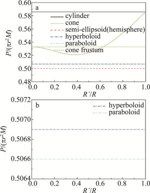
    Figure 3.  Minimum power radiated to the detector by frustum-of-cone shields with different R′/R

    因此,在所有形状的防辐射屏中,半球面防辐射屏自发辐射至探测器的功率最小,且与防辐射屏尺寸无关;其次为抛物面和双曲面,然后为台柱面,最大辐射功率为圆柱面防辐射屏。因此在实际应用中,将防辐射屏尽量设计为半球面,能最大程度减小其自发辐射对探测器的影响。

  • 以上讨论均为防辐射屏未开孔的情况,实际上为了从外部向探测器引入光、热等信号,还需要在防辐射屏顶部进行开孔。作者所设计的防辐射屏模型,开孔只需调整积分下限即可得到剩余部分对探测器的辐射功率。为减化讨论,这里只给出防辐射屏高度和底面半径相等、且未开孔辐射功率最小的防辐射屏开孔时的情况(其中台柱面防辐射屏上下端半径比为R′/R=0.38);开孔形状采用圆形,开孔半径为Rh(Rh < R)。

    不同形状防辐射屏顶部开不同尺寸孔后,剩余部分自发辐射至探测器的功率如图 4所示。可以看到,不同形状的防辐射屏在开孔尺寸相同时,圆柱面防辐射屏自发辐射至探测器的功率为所有形状中最大;抛物面和双曲面自发辐射至探测器的功率则始终几乎相等。开孔半径与底面半径之比为Rh/R < 0.27时,所有防辐射屏中自发辐射至探测器的功率最小的形状为半球面。而实际上对于超低温、单光子探测等应用,需要利用防辐射屏尽可能屏蔽环境杂散光,开孔尺寸会远小于该值,因此,前面对于半球面防辐射屏自发辐射至探测器的功率最小的结论仍然适用。

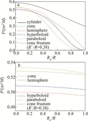
    Figure 4.  Spontaneous radiation power to the detector of different shields with varying-size holes on the top

  • 以上讨论的均是不同形状防辐射屏自发辐射至探测器的相对功率,为了进一步对比防辐射屏形状优化对超导单光子探测器自发辐射的切实改善情况,作者代入实际参数进行验证。不同形状防辐射屏在不同温度下单位时间自发辐射至探测器的光子数为:

    式中,P(λ)为防辐射屏自发辐射波长为λ的光至探测器的功率。假设防辐射屏内屏发射率η=0.1,探测器光敏区半径为r=25μm,则防辐射屏高度和底面半径相等时(对于台柱面,取上下端半径比R′/R=0.38),在3μm~12μm中远红外波段,不同形状防辐射屏在不同温度下单位时间自发辐射至探测器的光子数如表 1所示。

    shape of the shield temperature of the shield T/K
    60 70 80 90
    hemisphere 1.213×10⁴ 2.507×10⁵ 2.484×10⁶ 1.505×10⁷
    paraboloid 1.229×10⁴ 2.539×10⁵ 2.517×10⁶ 1.525×10⁷
    hyperboloid 1.230×10⁴ 2.541×10⁵ 2.518×10⁶ 1.526×10⁷
    cone frustum 1.263×10⁴ 2.611×10⁵ 2.588×10⁶ 1.568×10⁷
    cone 1.292×10⁴ 2.671×10⁵ 2.647×10⁶ 1.604×10⁷
    cylinder 1.421×10⁴ 2.937×10⁵ 2.910×10⁶ 1.763×10⁷

    Table 1.  Photon emission rate spontaneously radiated to the detector by di-fferent shapes of shields at different temperatures /Hz

    可见半球面防辐射屏自发辐射至探测器的中远红外光子数明显少于其它形状防辐射屏。以70K温度为例,此时半球面防辐射屏单位时间辐射至探测器的中远红外光子数比仅次于它的抛物面防辐射屏少3.2kHz,更是比常用的圆柱面防辐射屏少43kHz。防辐射屏温度更高和表面发射率更大时,采用半球面防辐射屏减少的自发辐射光子数会更加显著。

    综上所述,通过优化防辐射屏形状,能够明显减小防辐射屏自发辐射至探测器的光子数,从而减小由此引起的单光子探测器的伪计数率,提高探测器信噪比和灵敏度等性能。

3.   结论
  • 本文中系统研究了不同形状的防辐射屏自发辐射对探测器的影响。无论开小孔与否,在所有形状防辐射屏中,半球形防辐射屏自发辐射至探测器的功率最小;将防辐射屏形状优化至半球形,能够明显减小防辐射屏自发辐射至探测器的光子数,从而减小由其引起的单光子探测器的伪计数率,提高探测器性能。虽然只讨论了几种特殊形状的防辐射屏结构,而实际设计时要考虑的因素众多,防辐射屏很难完全按照某种单一形状进行配置,但本文中的研究结果依然能给防辐射屏设计提供有价值的参考。

Reference (22)

Catalog

    /

    DownLoad:  Full-Size Img  PowerPoint
    Return
    Return