Advanced Search

ISSN1001-3806 CN51-1125/TN Map

Volume 44 Issue 6
Nov.  2020
Article Contents
Turn off MathJax

Citation:

Surface damage study of silicon induced by combined millisecond and nanosecond laser with different delays

  • Received Date: 2019-12-12
    Accepted Date: 2019-12-20
  • The laser-silicon interaction process was investigated with the superposed radiation of two pulsed lasers. A pulse duration of 1ms was superposed by 7ns pulses, creating a combined pulse laser (CPL). The experimental study of single millisecond pulse laser and CPL irradiation on silicon wafer was carried out, respectively. Along with numerical calculation, the surface damage morphology caused by the two laser operation modes was compared. It can be divided into three kinds according to different delays of CPL. Further research was done on the melting depth and damage radius. The results show that the damage effect induced by CPL is more severe, including cleavage cracks, ablation and fold. The damage radius on the surface mainly depends on the energy density of incident ms laser, and the melting depth decreases with the increase of delay time. The better damage effect of CPL is ascribed to the pre-heating ms laser and the interaction of the follow-up ms laser with the surface damage formed by the ns laser. The results can be used as a reference for the processing of semiconductor materials by combined pulse laser in the future.
  • 加载中
  • [1]

    LI Z W, WANG X, SHEN Zh H, et al. Numerical simulation of millisecond laser-induced damage in silicon-based positive-intrinsic-negative photodiode[J]. Applied Optics, 2012, 51(14): 2759-2766. doi: 10.1364/AO.51.002759
    [2]

    LI Z W, WANG X, SHEN Zh H, et al. Mechanisms for the millisecond laser-induced functional damage to silicon charge-coupled imaging sensors[J]. Applied Optics, 2015, 54(3): 378-388. doi: 10.1364/AO.54.000378
    [3]

    ABBOTT M, COTTER J. Optical and electrical properties of laser texturing for high-efficiency solar cells[J]. Progress in Photovoltaics Research & Applications, 2006, 14(3): 225-235.
    [4]

    DANG C, LABIE R, TOUS L, et al. Investigation of laser ablation induced defects in crystalline silicon solar cells[J]. Energy Procedia, 2014, 55: 649-655. doi: 10.1016/j.egypro.2014.08.040
    [5]

    BASHIRI H, KARAMI M A, MOHAMMADNEJAD S. Improvement in IBC-silicon solar cell performance by insertion of highly doped crystalline layer at heterojunction interfaces[J]. Chinese Physics, 2017, B26(10): 108801.
    [6]

    BONSE J, BAUDACH S, KRVGER J, et al. Femtosecond laser ablation of silicon-modification thresholds and morphology[J]. Applied Physics, 2014, A74(1): 19-25.
    [7]

    BONSE J, BRZEZINKA K W, MEIXNER A J. Modifying single-crystalline silicon by femto-second laser pulses: An analysis by micro Raman spectroscopy, scanning laser microscopy and atomic force microscopy[J]. Applied Surface Science, 2004, 221(1/4): 215-230. doi: 10.1016/S0169-4332(03)00881-X
    [8]

    CROUCH C H, CAREY J E, WARRENDER J M, et al. Comparison of structure and properties of femtosecond and nanosecond laser-structured silicon[J]. Applied Physics Letters, 2004, 84(11): 1850. doi: 10.1063/1.1667004
    [9]

    DALILI A, TAN B, VRNKATAKRISHNAN K. Silicon wafer surface patterning using femtosecond laser irradiation below ablation threshold[J]. Optics and Lasers in Engineering, 2010, 48(3): 346-353. doi: 10.1016/j.optlaseng.2009.10.008
    [10]

    SIVAKUMAR M, TAN B, VENKATAKRISHNAN K. Enhancement of silicon nanostructures generation using dual wavelength double pulse femtosecond laser under ambient condition[J]. Journal of Applied Physics, 2010, 107(4): 044307. doi: 10.1063/1.3309422
    [11]

    ZHAO X, SHIN Y C. Ablation enhancement of silicon by ultrashort double-pulse laser ablation[J]. Applied Physics Letters, 2014, 105(11): 111907. doi: 10.1063/1.4896350
    [12]

    TAO H Y, CHEN R C, SONG X W, S, et al. Femtosecond laser pulse energy accumulation optimization effect on surface morphology of black silicon[J]. Acta Physica Sinica, 2017, 66(6): 067902(in Chinese).
    [13]

    MAO S S, MAO X L, GREIF R, et al. Simulation of infrared picosecond laser-induced electron emission from semiconductors[J]. Applied Surface Science, 1998, 127/129: 206-211. doi: 10.1016/S0169-4332(97)00633-8
    [14]

    THORSTENSEN J, FOSS S E. Temperature dependent ablation threshold in silicon using ultrashort laser pulses[J]. Journal of Applied Physics, 2012, 112(10): 103514. doi: 10.1063/1.4766380
    [15]

    CHAREE W, TANGWARODOMNUKUN V, DUMKUM C. Laser ablation of silicon in water under different flow rates[J]. The International Journal of Advanced Manufacturing Technology, 2014, 78(1/4): 19-29.
    [16]

    GALASSO G, KALTENBACHER M, TOMASELLI A, et al. A unified model to determine the energy partitioning between target and plasma in nanosecond laser ablation of silicon[J]. Journal of Applied Physics, 2015, 117(12): 1-6.
    [17]

    LI T, ZHOU C, LIU Z, et al. Computational and experimental study of nanosecond laser ablation of crystalline silicon[J]. International Communications in Heat and Mass Transfer, 2011, 38(8): 1041-1043. doi: 10.1016/j.icheatmasstransfer.2011.05.010
    [18]

    SUN W, QI H, FANG Z, et al. Nanosecond laser pulse induced concentric surface structures on SiO2 layer[J]. Optics Express, 2014, 22(3): 2948-2954. doi: 10.1364/OE.22.002948
    [19]

    WANG X, QIN Y, WANG B, et al. Numerical and experimental study of the thermal stress of silicon induced by a millisecond laser[J]. Applied Optics, 2011, 50(21): 3725-3732. doi: 10.1364/AO.50.003725
    [20]

    CHOI S, JHANG K Y. Initiation time of near-infrared laser-induced slip on the surface of silicon wafers[J]. Applied Physics Letters, 2014, 104(25): 251604. doi: 10.1063/1.4885385
    [21]

    CHOI S, JHANG K Y. In situ detection of laser-induced slip initiation on the silicon wafer surface[J]. Optics Letters, 2014, 39(14): 4278-4281. doi: 10.1364/OL.39.004278
    [22]

    JIA Z Ch, LI Z W, ZHOU J, et al. Slip on the surface of silicon wafers under laser irradiation: Scale effect[J]. Chinese Physics, 2017, B26(11): 116102.
    [23]

    WANG B, QIN Y, NI X W, et al. Effect of defects on long-pulse laser-induced damage of two kinds of optical thin films[J]. Applied Optics, 2010, 49(29): 5537-5544. doi: 10.1364/AO.49.005537
    [24]

    DONNELLY T, LUNNEY J G, AMORUSO S, et al. Double pulse ultrafast laser ablation of nickel in vacuum[J]. Journal of Applied Physics, 2009, 106(1): 013304. doi: 10.1063/1.3159010
    [25]

    SALLEO A, SANDS T, GÉNIN F Y. Machining of transparent materials using an IR and UV nanosecond pulsed laser[J]. Applied Physics, 2000, A71(6): 601-608.
    [26]

    HATANO M, MOON S, LEE M, et al. Excimer laser-induced temperature field in melting and resolidification of silicon thin films[J]. Journal of Applied Physics, 1999, 87(1): 36-43. doi: 10.1152/jappl.1999.87.1.36
    [27]

    TAKASUKA E, TOKIZAKI E, TERASHIMA K, et al. Emissivity of liquid silicon in visible and infrared regions[J]. Journal of Applied Physics, 1997, 81(9): 6384-6389. doi: 10.1063/1.364418
    [28]

    LV X M, PAN Y X, JIA Z Ch, et al. Surface damage induced by a combined millisecond and nanosecond laser[J]. Applied Optics, 2017, 56(17): 5060-5067. doi: 10.1364/AO.56.005060
    [29]

    RAVINDRA N M, RAVINDRA K, MAHENDRA S, et al. Modeling and simulation of emissivity of silicon-related materials and structures[J]. Journal of Electronic Materials, 2003, 32(10): 1052-1058. doi: 10.1007/s11664-003-0088-0
    [30]

    LI Z W, ZHANG H Ch, SHEN Z H, et al. Time-resolved temperature measurement and numerical simulation of millisecond laser irradiated silicon[J]. Journal of Applied Physics, 2013, 114(3): 033104. doi: 10.1063/1.4815872
    [31]

    CHOI S, JHANG K Y. Thermal damages on the surface of a silicon wafer induced by a near-infrared laser[J]. Optical Engineering, 2014, 53(1): 017103. doi: 10.1117/1.OE.53.1.017103
    [32]

    WANG X, QIN Y, LI Z W, et al. The interaction and the surface crack of single-crystal silicon induced by a millisecond laser[J]. Laser Physics, 2012, 22(10): 1627-1634. doi: 10.1134/S1054660X12100234
    [33]

    WANG X, SHEN Zh H, LU J, et al. Laser-induced damage threshold of silicon in millisecond, nanosecond, and picosecond regimes[J]. Journal of Applied Physics, 2010, 108(3): 033103. doi: 10.1063/1.3466996
    [34]

    MAO X L, CHAN W T, CAETANO M, et al. Preferential vaporization and plasma shielding during nano-second laser ablation[J]. Applied Surface Science, 1996, 96/98: 126-130. doi: 10.1016/0169-4332(95)00420-3
    [35]

    PAN Y X, LV X M, ZHANG H Ch, et al. Millisecond laser machining of transparent materials assisted by a nanosecond laser with different delays[J]. Optics Letters, 2016, 41(12): 2807-2810. doi: 10.1364/OL.41.002807
    [36]

    WANG X, ZHU D H, SHEN Zh H, et al. Surface damage morphology investigations of silicon under millisecond laser irradiation[J]. Applied Surface Science, 2010, 257(5): 1583-1588. doi: 10.1016/j.apsusc.2010.08.098
  • 加载中
通讯作者: 陈斌, bchen63@163.com
  • 1. 

    沈阳化工大学材料科学与工程学院 沈阳 110142

  1. 本站搜索
  2. 百度学术搜索
  3. 万方数据库搜索
  4. CNKI搜索

Figures(5)

Article views(9068) PDF downloads(20) Cited by()

Proportional views

Surface damage study of silicon induced by combined millisecond and nanosecond laser with different delays

  • 1. Department of Intelligent Equipment, Changzhou College of Information Technology, Changzhou 213000, China
  • 2. School of Science, Nanjing University of Science & Technology, Nanjing 210094, China
  • 3. State Key Laboratory of Laser Interaction with Matter, Northwest Institute of Nuclear Technology, Xi'an 710024, China

Abstract: The laser-silicon interaction process was investigated with the superposed radiation of two pulsed lasers. A pulse duration of 1ms was superposed by 7ns pulses, creating a combined pulse laser (CPL). The experimental study of single millisecond pulse laser and CPL irradiation on silicon wafer was carried out, respectively. Along with numerical calculation, the surface damage morphology caused by the two laser operation modes was compared. It can be divided into three kinds according to different delays of CPL. Further research was done on the melting depth and damage radius. The results show that the damage effect induced by CPL is more severe, including cleavage cracks, ablation and fold. The damage radius on the surface mainly depends on the energy density of incident ms laser, and the melting depth decreases with the increase of delay time. The better damage effect of CPL is ascribed to the pre-heating ms laser and the interaction of the follow-up ms laser with the surface damage formed by the ns laser. The results can be used as a reference for the processing of semiconductor materials by combined pulse laser in the future.

引言
  • 半导体是光电探测器的基础材料[1-2],并且在微电子和太阳能电池领域有着重要的应用[3-5]。硅是地球上第二丰富的元素,它作为一种典型的半导体材料,被广泛应用于各个领域。前人对这种材料的激光辐照效应进行了广泛的研究,激光辐照硅及硅基材料时,会产生解理断裂、熔化和汽化等不可逆损伤。因此,研究激光波长、脉宽、脉冲数量等因素对其损伤形貌的影响具有重要意义。而大多数研究都是针对单束脉冲激光(脉宽包括飞秒[6-12]、皮秒[13-14]、纳秒[15-18]、毫秒[19]等)和连续激光[20-22]。到目前为止,关于组合脉冲激光辐照致硅材料损伤形貌的研究还很少。

    一般来说,半导体在激光辐照下的表面损伤形貌具有粗糙表面、激光诱导的周期性表面结构以及熔化再凝固形成的非晶态等特征。例如,BONSE等人[7]研究了单束飞秒激光对单晶硅的表面改性,发现了几种不同的表面形貌结构(边缘和突起),并讨论了它们的形成原因。SUN等人[18]报道了波长为1.06μm的单束纳秒脉冲激光辐照SiO2层时表面产生的周期性同心结构,并进一步研究了激光能量密度对该结构的条纹周期、损伤部位大小和深度的影响。关于双脉冲激光的研究也有不少。比如,SIVAKUMAR等人[10]提出了一种在空气环境下利用双波长双脉冲飞秒激光辐照增加网状硅纳米纤维结构形成的独特方法。ZHAO等人[11]通过建立原子模拟模型,分析了延迟时间对飞秒双脉冲激光烧蚀硅的影响,发现在总的脉冲能量相等的情况下,与单脉冲相比,双脉冲烧蚀能显著提高对硅的烧蚀效率。

    然而,上述研究并未涉及组合脉冲激光辐照硅材料产生表面形貌的研究。毫秒激光因其具有脉冲持续时间长、能量大等优点,在激光加工工业中应用广泛,能量耦合效率高[23]。而高功率密度的纳秒脉冲激光辐照很容易造成材料表面的损伤,尽管相互作用过程中会产生空气击穿和等离子体[24]。SALLEO等人[25]指出, 有两种办法可以有效提高加工效率,一是采用材料吸收更强的短波长激光,二是在样品上激光作用的位置引入缺陷来增加对激光的吸收。考虑到在激光有效作用过程中,不仅需要激光能量的累积,还需要高峰值功率,因此, 本文中采用了在毫秒脉冲激光作用过程中增加一束脉宽为纳秒的脉冲激光叠加作用的组合方式,简称为组合脉冲激光。本文中通过实验研究了单晶硅材料在两种激光工作模式(单束毫秒脉冲激光和组合脉冲激光)辐照下的表面损伤形貌;讨论了组合脉冲激光辐照单晶硅材料时不同延迟时间对熔融深度和表面损伤半径的影响;最后,在实验结果和前人研究的基础上,分析了组合脉冲激光辐照硅材料的损伤机理。

1.   实验装置
  • 实验装置如图 1所示。毫秒激光器采用镭宝公司Meyer-50激光器,其脉宽0.5ms~2.5ms可调(本文中所用1ms),最大激光输出能量50J。纳秒激光器为镭宝公司DAWA-200激光器,脉宽7ns,最大输出能量200mJ。两束激光的波长1064nm,以TEM00模式输出,空间分布呈近高斯分布。两束输出激光束通过聚焦透镜L1(f=125mm)聚焦于样品,调整透镜位置,使得光斑半径均为1.1mm。(100)单晶硅靶材(厚度0.5mm)放置在3维平移台上。实验前,硅片经过异丙醇和去离子水清洗后,再用HF溶液去了氧化层,最后再经去离子水清洗一遍。入射激光的能量大小可以由衰减片和分束器调节,并由能量计实时记录。此外,还利用PIN光电二极管实时检测入射激光的散射信号。图 1中BS为分光镜,M1和M2为反光镜,PBS为偏振分光棱镜。

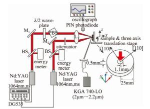
    Figure 1.  Schematic diagram of experimental setup

    实验中靶材表面温度可以通过一台高速红外测温仪记录(型号为KGA 740-LO,该测温仪发射率0.1~1可调,响应时间为6μs,最小取样时间间隔为10μs,感光频谱范围为2μm~2.2μm,温度记录范围350℃~3500℃)。在激光辐照过程中,整个硅片的温度是非均匀且不断变化的,发射率也会随之不断改变[26]。而液态硅的发射率随温度变化较小,因此红外测温仪的发射率设定为波长2μm~2.2μm范围内的平均值0.17[27]。两束脉冲激光的延迟时间Δt定义为探测得到的毫秒脉冲激光信号的上升沿与纳秒脉冲激光信号峰值之间的时间间隔,可以通过DG535数字延迟发生器控制。当纳秒脉冲激光在毫秒脉冲激光之前激发时,该值为负值。

2.   结果与讨论
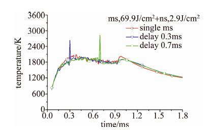
  • 根据实验中单束毫秒脉冲激光和组合脉冲激光分别辐照测得的结果,图 2中给出了靶材表面中心点的温度变化情况。延迟时间分别取了0.3ms和0.7ms,两束脉冲激光的能量密度分别为69.9J/cm2和2.9J/cm2,选取原因在之前的工作中已经有相关解释[28]。相比之下,这两种激光工作模式引起的温升过程较为相似,除了组合脉冲激光辐照过程中发生的突变。即使靶材表面仍被毫秒脉冲激光辐照,但纳秒脉冲激光的辐照会在很短时间内(微秒量级)造成剧烈温升,随后温度迅速降低。这是因为毫秒脉冲激光的功率密度远小于纳秒脉冲激光。

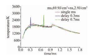
    Figure 2.  Temperature evolution at the center point of sample surface under the two laser operation modes

    实际上,纳秒脉冲激光辐照过程中温度可以达到气化点。但实验过程中红外测温仪将硅的发射率设成了固定值0.17,而硅的实际发射率会随着温度的改变而改变[29]。此外,红外测温仪的最小采样时间是10μs,所以只能得到纳秒脉冲激光辐照过程中温升的近似趋势。在参考文献[30]中该红外测温仪的测量原理和曲线分析有更详细的解释,比如温升曲线中产生的峰和谷。

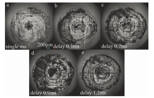
  • 实验中硅靶材的表面损伤形貌可以通过光学显微镜观察得到。如图 3a所示,该表面损伤是由能量密度为69.9J/cm2的单毫秒脉冲激光辐照造成的。激光辐照后靶材表面中心产生了明显的熔坑,表面出现了解理裂纹,且都沿〈110〉和〈110〉晶向分布[31],连续不断的贯穿整个重凝区域。根据参考文献[32]中的结果,辐照区域的温升会导致热膨胀,而材料的连续性会阻碍其自由膨胀,从而产生热应力。在凝固过程中,辐照区域的热应力由压应力逐渐转变为拉应力。当拉伸应力超过材料的拉伸强度时,会产生表面裂纹,且都分布在激光照射区域内。在之前的研究中也通过数值计算获得了相应的热应力变化情况[28],该损伤形貌与之前的结果较为吻合。

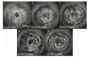
    Figure 3.  Surface damage morphology induced by two different laser operation modes

    图 3b~图 3e中给出了不同延迟时间的组合脉冲激光辐照硅靶材时造成的表面损伤形貌。考虑不同的损伤效应和图 2中的温度变化情况,与图 3a相比,可以将它们分为3种:(1)纳秒脉冲激光在靶材表面未完全熔化前开始辐照,如图 3b所示, 与图 3a相比,图 3b中出现了明显的烧蚀区域;(2)纳秒脉冲激光在靶材表面完全熔化之后开始辐照,如图 3c图 3d所示,靶材表面中心处的熔坑逐渐扩大,烧蚀区域面积增大但烧蚀深度变浅,损伤区域边缘能明显看到熔融产物凝固之后形成的皱褶,并且部分解理条纹被覆盖;(3)纳秒脉冲激光在毫秒脉冲激光辐照结束之后开始辐照,如图 3e所示,毫秒脉冲激光辐照结束后靶材冷却过程中表面会出现解理条纹,此时靶材表面表现出脆性。在纳秒脉冲激光辐照下,靶材表面会形成更加明显的烧蚀区域,覆盖一部分解理条纹,甚至对表面产生的冲击力会造成块状表层的脱落。

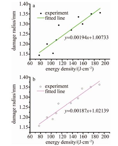
    从损伤形貌上可以看出,组合脉冲激光对靶材表面的损伤效果更为显著,且延迟时间的变化也会产生不同的影响。因此,本文中进一步研究了激光辐照后靶材表面损伤半径和熔融深度的变化情况。图 4是根据实验结果获得的靶材表面损伤半径随激光能量密度的变化关系。与毫秒脉冲激光相比,纳秒脉冲激光的能量密度较低,热影响范围和热扩散深度较小[33],因此, 分析过程中仅考虑了损伤半径随毫秒脉冲激光能量密度的变化情况。通过图 4a图 4b中的线性拟合发现,单毫秒脉冲激光和组合脉冲激光作用结果的曲线趋势近似,即:随着入射激光能量密度的增加,损伤半径逐渐增大,并且两种情况下的斜率近似。这说明在这两种激光工作模式下,靶材表面的损伤半径主要与毫秒脉冲激光的能量密度有关。

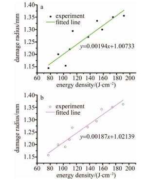
    Figure 4.  Surface damage radius vs. incident energy density of the ms laser

    图 5是组合脉冲激光辐照硅靶材时熔融深度和损伤半径随延迟时间的变化曲线。由于实验条件的限制,熔融深度可以通过数值模型[28]计算得到。从图中可以发现,表面损伤半径一直保持在1.1mm左右,延迟时间的变化对损伤半径的影响较弱,这也侧面验证了损伤半径主要依赖于入射毫秒脉冲激光能量密度的大小。纳秒脉冲激光辐照造成的表面烧蚀将增加靶材表面的粗糙度,而较小的延迟时间意味着纳秒脉冲激光辐照结束后,毫秒脉冲激光的剩余辐照时间较长,这会进一步提高靶材对毫秒脉冲激光能量耦合的效率。但随着延迟时间的延长,靶材表面将逐渐熔化,这将导致更高的表面反射率[30],甚至会出现蒸汽或等离子屏蔽[34]。因此,与损伤半径变化趋势不同,熔融深度会随延迟时间的改变而发生较大变化:当延迟时间大于零后,它会随着延迟时间的增大而逐渐减小。这个趋势与PAN等人的研究结果相吻合[35]

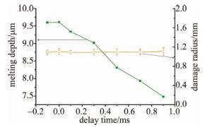
    Figure 5.  Change of melting depth and damage radius with different delays of CPL

  • 组合脉冲激光和单毫秒脉冲激光辐照对硅靶材造成的表面损伤有许多不同之处,这是不同脉宽的脉冲激光损伤机制不同所导致的。在本文实验中,热损伤是毫秒脉冲激光的主要损伤机制,而表面烧蚀和应力损伤则是由纳秒脉冲激光辐照造成的[36]。从表面损伤形貌的角度来说,组合脉冲激光的损伤效应更为严重,且不同的延迟时间造成的损伤效应也不相同。原因之一是毫秒脉冲激光的预加热效应:在毫秒脉冲激光辐照预加热下,靶材表面温度升高,硅的吸收系数将逐渐增大。同时靶材表面变软,材料屈服强度大大降低。因此,靶材在纳秒脉冲激光辐照下更容易产生表面损伤,包括烧蚀、反冲压力和应力损伤。另一个原因与后续毫秒脉冲激光和纳秒脉冲激光造成的表面损伤相互作用有关。纳秒脉冲激光造成的表面损伤会增加表面粗糙度,从而增大了靶材对后续毫秒脉冲激光能量的吸收,进一步加剧表面损伤。

    但是延迟时间较长时,在纳秒脉冲激光辐照之前靶材表面中心区域已经部分熔化,液态硅的表面反射率较高,会导致激光能量的耗散。不过在这样的情况下,靶材会在纳秒脉冲激光的辐照下更容易达到更高温度,甚至会发生汽化、飞溅甚至等离子体现象,这在本文中没有讨论。

3.   结论
  • 通过实验测量获得了单束毫秒脉冲激光和组合脉冲激光分别辐照下硅靶材表面的温升情况,并比较了这两种激光模式造成的靶材表面损伤形貌。研究发现, 组合脉冲激光造成的损伤效应更为严重,根据延迟时间的不同,表面损伤形貌可分为3种。进一步研究表明,表面损伤半径主要取决于入射毫秒脉冲激光的能量密度,延迟时间对它的影响较小,而熔融深度会随着延迟时间的增加而减小。讨论了组合脉冲激光辐照硅靶材的损伤机理,组合脉冲激光损伤效果的增强主要与毫秒脉冲激光的预加热效应以及纳秒脉冲激光造成的表面损伤与后续毫秒脉冲激光的相互作用有关。本文中的研究结果可为今后组合脉冲激光加工半导体材料提供参考。

Reference (36)

Catalog

    /

    DownLoad:  Full-Size Img  PowerPoint
    Return
    Return