 Map
Map


HTML
-
近年来,随着网络技术的快速发展,人们对网络传输容量的需求越来越高。传统的掺铒光纤放大器由于工作带宽较窄且主要工作在C+L波段,极大地限制了光纤通信系统的带宽,难以满足高速度和大容量的通信要求。因此,研究覆盖1100nm~1700nm全波段的高效有源光纤材料已成为该领域的研究热点。
为了增加光纤通信系统的传输带宽,人们研究了多种光纤放大器和激光器增益介质,主要包括:各种稀土元素(Yb3+,Nb3+,Pr3+,Tm3+,Ho3+等)、过渡金属元素(Cr3+,Cr4+,Ni2+等)和主族元素(Tl0,Pb+,Pb0,Bi等)。研究发现,掺铋玻璃和光纤的辐射波长可以覆盖1100nm~1700nm[1-5],荧光寿命可以达到几百微秒,因此它被认为是最有发展前景的近红外(near-infrared, NIR)荧光材料之一。随着无水光纤制备技术的发展,基于化学沉积技术制成的掺铋光纤更具备实用前景,有望在使用单波长抽运源的抽运下实现位于1100nm~1700nm波段的超宽带激光发射和光放大。因此,掺铋光纤可用作超宽带光纤放大器和激光器的新型增益介质,以弥补传统掺稀土离子放大器和激光器的不足。
铋原子的电子结构为[Xe]4f145d106s26p3,其壳外电子处于半满状态,这意味着壳外电子较为活跃。因此,铋原子对基质材料极其敏感,易于形成各种价态的离子,例如Bi0, Bi+, Bi2+, Bi3+和Bi5+。铋离子价态的多样性使得掺铋光纤的发光机理变得更加复杂。近年来,为掌握其发光机理,科研人员对掺铋光纤进行了大量研究,并提出了许多关于铋活性中心的假设。在本文中,将系统介绍这些铋活性中心的结构和发光特性,为研制高性能的掺铋材料提供理论指导。由于铋离子的价态会极大地影响铋活性中心的性能,根据铋的价态将铋活性中心分为高价态铋中心、低价态铋中心、间隙铋中心。
-
2001年,FUJIMOTO等人[3]首次发现了掺铋玻璃的近红外发光现象,他们在500nm抽运光下测试了掺铋玻璃的发光光谱,发现在室温下该材料的发光峰位于1400nm。他们认为发光中心是高价态Bi5+离子,该发光可能是由Bi5+离子从激发态3D3, 2, 1跃迁到基态1S0而产生的。为了证明发光中心是Bi5+离子,他们研究了铋离子周围的局部结构,发现Bi和O之间的距离为0.23nm[6]。
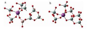
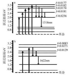
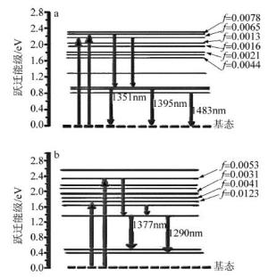
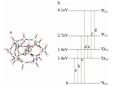
2013年,WEN等人[7]采用基于量子化学的密度泛函理论计算了掺铋光纤中Bi5+离子的发光特性。图 1中给出了有Al掺杂的Bi5+模型和没有Al掺杂的Bi5+模型的局部结构。图 2a是有Al掺杂的Bi5+模型的能级图, 图中f是振子强度。激发能级依次为2.0023eV, 2.5044eV, 2.9067eV, 3.0201eV和3.1673eV,第四激发态的电子辐射到更低能级,会产生位于第二通信窗口范围内的1318nm发光。图 2b是没有Al掺杂的Bi5+模型能级图。在2.5009eV和2.8483eV能量的激发下,第三激发态的电子会辐射产生1622nm的发光,然而这一发光不在第二通信窗口范围内。
上述研究表明,掺铋光纤近红外发光可能是含Al的高价铋中心产生的。但大量实验表明,随着基质碱度的增加,掺铋玻璃的NIR发光强度变弱[8-10]。其次,掺铋光纤的制备过程需要高温处理,铋元素更可能以低价态的形式存在[11]。另外,增加还原剂会增加掺铋光纤的NIR发光强度,而增加氧化剂则会降低NIR发光强度[12]。因此,研究人员普遍认为高价态铋是不稳定的发光中心,低价态铋中心和间隙铋中心等才是掺铋光纤近红外发光的起源。

-
2013年,SOKOLOV等人[13]应用第一性原理研究了掺铋SiO2和GeO2玻璃中的铋活性中心。在三配位Bi中心中,Bi原子与3个O原子成键,Bi-O键长为0.213nm,O-Bi-O键角为94.6°。而在四配位Bi中心中,Bi-O键长分别为0.209nm和0.230nm,O-Bi-O键角分别为92.2°和160.8°。他们认为吸收波长和发光波长受制于基质材料。在SiO2中,三配位Bi原子的吸收带是0.26μm,四配位Bi原子的吸收带是0.22μm。而在GeO2中,三配位Bi原子和四配位Bi原子的吸收带分别是0.24μm和0.23μm。在上述吸收带的激发下,发光波长可以达到0.3μm~0.4μm。
2013年,WEN等人[7]还研究了掺铋光纤中Bi3+离子的发光特性。图 3a是有Al掺杂的Bi3+模型的能级图。基态电子被激发到2.17eV和2.25eV两个不同的激发态,激发态的电子跃迁回基态时,会产生1483nm,1395nm和1351nm的发光。图 3b是没有Al掺杂的Bi3+模型的能级图。基态电子被激发到2.35eV和1.74eV两个不同的激发态,第三激发态的电子跃迁到第一和第二激发态时,分别发出1290nm和1377nm的荧光。在Bi3+-Al共掺情况下,振子强度都相对较低,但在没有Al掺杂的Bi3+模型中,存在着振子强度为0.0123的激发态。因此,他们指出没有Al掺杂的Bi3+模型是近红外发光的主要原因。
2018年,作者所在团队研究了掺铋石英光纤中环状结构对Bi3+离子发光特性的影响[14]。通过构建3元环~6元环(member ring, MR)Bi3+离子团簇模型,来研究环状结构对光纤发光的作用。在Bi3+团簇模型中,Bi-O键的平均键长为0.204nm,O-Bi-O平均键角为95.8°。表 1中给出了不同环状结构的Bi3+离子吸收和发光特性。可发现1S0→1P1跃迁的吸收波长通常小于250nm,与参考文献[15]、参考文献[16]中的实验值一致,而且不受环状结构的影响。在3MR,4MR,5MR和6MR中1P1→1S0的荧光分别约为463nm,374nm,352nm和343nm; 而对应的3P1→1S0磷光分别约为665nm,516nm,391 nm和358nm.这实际上说明了Bi3+离子掺杂光纤可以实现从紧紫外到可见光的宽光谱发光。
吸收
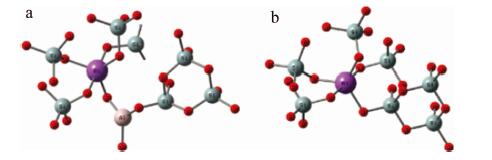
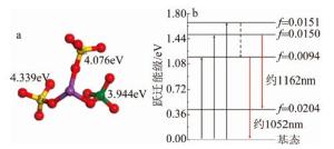
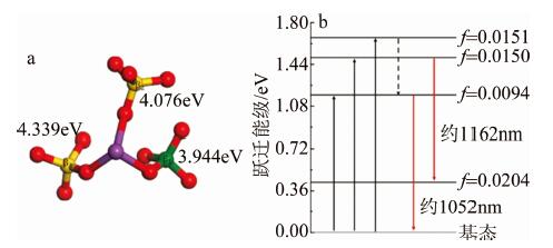
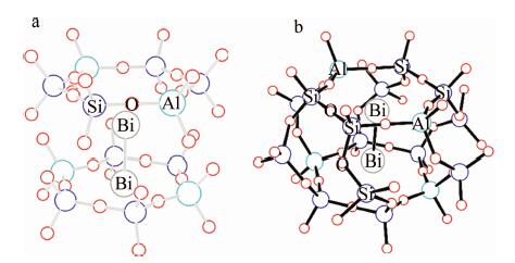
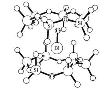
1S0→1P1/nm发光 1P1→1S0/nm 3P1→1S0/nm Bi-3MR 229 463 665 Bi-4MR 224 374 516 Bi-5MR 231 352 391 Bi-6MR 227 343 358 2019年,作者所在团队利用第一性原理计算了Bi/Al共掺石英光纤模型的几何结构和光学性质[17]。图 4a为Bi/Al共掺模型的局部结构。Al原子倾向于取代Bi-O-Si模型中Si原子的位置,Bi-O键长的平均值为0.215nm,O-Bi-O键角的平均值是98.86°,Al原子的掺入降低了Bi3+发光中心的结构聚合度。图 4b是Bi/Al共掺模型的能级图。电子从基态被激发到1.18eV, 1.48eV和1.77eV的激发态,被激发的电子通过非辐射跃迁到第二和第三激发态,辐射发出波长约为1052nm和1162nm的荧光,与实验发现的Bi/Al共掺光纤存在约1100 nm发光吻合[3, 18-19]。
-
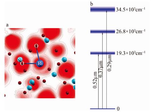
2013年,SOKOLOV等人[13]还研究了掺铋SiO2和GeO2玻璃中的2价Bi替代中心。在GeO2中,二配位Bi原子不能稳定存在,会转换成三配位Bi原子。在SiO2中,Bi原子通过桥接O原子形成二配位Bi原子,如图 5a所示。他们还计算了2价Bi替代中心的能级和跃迁性质,如图 5b所示,Bi2+离子模型的吸收带分别是0.52μm, 0.37μm和0.29μm,考虑到2价Bi替代中心的斯托克斯位移比较大,Bi2+离子模型能够产生0.6μm~0.7μm范围内的发光。

2018年,作者所在团队研究了掺铋石英光纤中不同环状结构对Bi2+替换中心的影响[20]。在3MR~6MR模型中,Bi-O键的平均键长为0.211nm,O-Bi-O键角的平均值为96.74°。还计算了3MR~6MR中Bi2+离子的能级和吸收带,如表 2所示。在3MR~6MR模型中,Bi2+离子的2P1/2→2P3/2(1)跃迁对应的吸收带分别为503.86nm, 473.35nm, 461.24nm和469.31nm,由2P1/2→2P3/2(2)的跃迁则会产生377.71nm, 445.21nm, 417.33nm和411.55nm的吸收带,299.63nm, 309.42nm, 322.47nm和302.45nm的吸收带归因于Bi2+离子的2P1/2→2S1/2跃迁。由此可见,掺铋光纤中的红色发光是由Bi2+离子的2P3/2(1)→2P1/2的跃迁产生的,而且3MR模型中Bi2+离子的跃迁是产生红色发光的主要原因[21]。
结构 能级/103cm-1 波长λab/nm 3MR 0 19.86 26.47 33.37 299.63 377.71 503.86 4MR 0 21.12 22.46 32.31 309.42 445.21 473.35 5MR 0 21.68 23.96 31.01 322.47 417.33 461.24 6MR 0 21.31 24.30 33.06 302.45 411.55 469.31 Bi2+参考值 0 19.3 26.8 34.5 290 370 520 -
2005年,MENG等人[22]首次提出掺铋光纤的近红外发光中心可能是Bi+离子。由于自旋轨道耦合作用,Bi+(6s26p2)离子将分裂为3P0基态和1S0, 1D2, 3P2,1激发态。他们把掺铋铝硅酸盐玻璃中500nm, 700nm, 800nm和1000nm的吸收带归因于Bi+离子的基态3P0到激发态1S0, 1D2, 3P2,1之间的跃迁,产生的近红外发光则是由Bi+离子的3P1→3P0导致的。
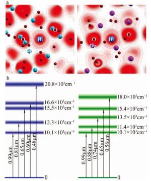
2013年,SOKOLOV等人[13]还计算了掺铋SiO2和GeO2模型中间隙Bi+离子的能级和跃迁情况,间隙Bi+离子的电子密度图和能级图分别如图 6a和图 6b所示。Bi+离子的基态3P0,不受晶体场影响。第一激发态3P1,受轴向晶场的影响会分裂成两个能级。第二激发态3P2,被分裂成3个能级。3P1能级在SiO2中约为10100cm-1和12300cm-1,在GeO2中约为10100cm-1和11400cm-1。3P2能级在SiO2中约为15500cm-1, 16600cm-1和20800cm-1,在GeO2中为13500cm-1, 15400cm-1和18000cm-1。
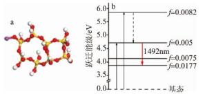
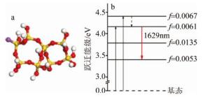
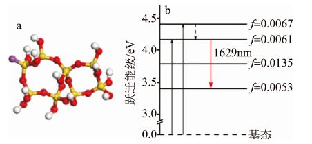
2018年,作者所在团队研究了掺铋光纤中单价铋的近红外发光特性[23]。图 7a和图 8a是Bi+离子团簇结构模型。SiOBi结构的形成能相对SiBi结构要低,更容易形成。在SiOBi模型中,Bi-O键长为0.211nm,Bi-O-Si的平均键角约为127.5°。在SiBi模型中,Si-Bi键长为0.267nm,Bi-Si-O键角为127.5°。同时计算了SiOBi与SiBi结构的能级图,如图 7b和图 8b所示。在SiOBi结构中,基态电子可以被激发到5.856eV和4.704eV两个不同的能级,第三激发态的电子跃迁到第一激发态时,辐射发出1492nm的荧光,与参考文献[24]中报道的1450nm发光很接近。在SiBi结构中,激发能级分别为4.406eV和4.163eV,第三激发态的电子跃迁到第一激发态时,辐射发出1629nm的荧光。
2.1. 3价铋中心

2.2. 2价铋中心
2.3. 1价铋中心


-
2005年,PENG等人[25-26]提出了掺铋石英玻璃中NIR发光机理的另一种解释。他们认为NIR发光中心很可能是由Bi原子或多个Bi原子形成的团簇所引起的。因为Bi2O3在高温下容易分解并且会进一步分解成Bi原子。近年来,SOKOLOV等人[13, 27-29]和作者所在团队[30]通过第一性原理计算,发现间隙Bi原子和间隙Bi二聚体可能是掺铋光纤近红外发光的起源。此外,间隙Bi氧化物分子[23, 31]也被认为是掺铋光纤近红外发光中心。
-
2013年,SOKOLOV等人[27]计算了铝硅酸盐玻璃中间隙Bi0原子的光学性质。图 9a中给出了间隙Bi0原子的结构模型。Bi0原子的平衡位置在两个六环之间,并且铋原子不与周围原子成键,结构非常稳定。图 9b中给出了间隙Bi0原子的能级图。间隙Bi0原子产生的吸收带在不大于400nm,约500nm, 600nm~700nm和900nm~1100nm范围内,该吸收可以产生1000nm~1300nm和1400nm~1600nm范围内的近红外发光。随后,SOKOLOV等人[13]研究了掺铋SiO2和GeO2玻璃中间隙Bi0原子的存在情况,图 10是间隙Bi0原子的电荷密度图。间隙Bi0原子与周围原子相互作用弱,不和其它原子成键,可以在6MR间隙位置稳定存在。间隙Bi0原子的基态是4S3/2,第一激发态和第二激发态分别为2D3/2和2D5/2,轴向晶体场可以使这些激发态产生分裂。间隙Bi0原子的第三激发态2P1/2,不能被静电场分裂。他们把不大于0.4μm范围内相对较强的吸收带,归因于间隙Bi0原子的4S3/2→2P1/2跃迁。

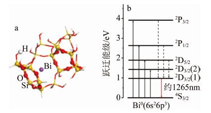
2019年,作者所在团队研究了掺铋石英光纤中间隙Bi0原子的光学性质[30]。图 11a中给出了间隙Bi0原子团簇模型。间隙Bi0原子最可能存在于距离6MR中心约0.2nm处,并与其周围原子相互作用很弱。图 11b是间隙Bi0原子的能级图。以约为317nm, 472nm, 657nm和865nm为中心的吸收带主要归因于间隙Bi0原子4S3/2→2P3/2, 4S3/2→2P1/2, 4S3/2→2D5/2和4S3/2→2D3/2(2)的跃迁。此外,约1265nm的近红外发光被认为是间隙Bi0原子的2D3/2(1)→4S3/2跃迁引起的, 与参考文献[26, 32-33]中报道的结果一致。

-
2008年,SOKOLOV等人[28]研究了铝硅酸盐结构中间隙Bi2二聚体的近红外发光特性。他们构建了Bi2, Bi2-和Bi22-二聚体模型,如图 12a所示。中性Bi2二聚体沿元环轴向排列,Bi原子位于元环平面的两侧。当一个或两个额外电子添加到团簇结构,会在两个六元环间隙位置形成Bi2-或Bi22-二聚体结构。他们认为在铝硅酸盐玻璃网络中,间隙Bi2-和Bi22-二聚体会更加稳定且是近红外发光的中心。2009年,SOKOLOV等人[29]研究了掺铋铝硅酸盐玻璃中间隙Bi2二聚体的稳定性,主要包括中性二聚体Bi2和负二聚体Bi2-和Bi22-,如图 12b所示。同时对间隙Bi2二聚体的电子光谱、喇曼光谱、电子自旋共振和发光特性进行了详细研究,他们也认为Bi2-和Bi22-二聚体是掺铋玻璃中近红外发光的中心。

-
2011年,SOKOLOV等人[31]提出间隙BiO分子可能是掺铋石英玻璃近红外发光中心,并给出了间隙BiO分子模型图,如图 13所示。在SiO2网络中,BiO分子可以存在于两个6MR之间,并沿6MR结构的轴向排列,BiO分子偏差或位移不会对周围环境造成任何改变,因此这种结构是稳定的。通过对比实验结果,他们认为近红外发光的原因是由于掺铋SiO2玻璃中存在间隙BiO分子。

-
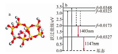
2018年,作者团队还计算了掺铋光纤中间隙Bi2O结构的发光特性[23]。间隙Bi2O模型如图 14a所示,Bi2O分子存在于6MR的间隙位置,并且沿着6MR结构的轴向排列,Bi-O键长分别为0.2117nm和0.2116nm,Bi-O-Bi键角为144.3°。还计算了间隙Bi2O结构的能级图,如图 14b所示,间隙Bi2O结构具有1.082eV, 1.966eV, 3.181eV和3.421eV等一系列不同的激发能级,由于较高的振子强度,对应的发光寿命相对较长。第二激发能级的电子将辐射跃迁到较低能级,产生1403nm和1147nm的发光,与先前的实验结果[16, 34]吻合较好。

3.1. 间隙铋原子

3.2. 间隙Bi2二聚体
3.3. 间隙BiO分子
3.4. 间隙Bi2O分子
-
目前,虽然对于掺铋光纤的发光机理没有明确的结论,但经过近几年的研究,研究人员普遍认为高价态铋不可能是掺铋光纤近红外发光的起源,掺铋光纤近红外发光的起源更偏向于低价态铋、间隙铋中心等结构。铋元素的发光机理研究是当前迫切需要解决的难题,只有彻底掌握其发光机理,才能针对性地研制出高效率高性能的掺铋材料。本文中系统地整理了掺铋光纤发光机理的系列研究成果,从铋活化中心的结构和发光特性出发,总结了掺铋光纤中不同结构与发光波长之间的关系。此工作将为掺铋光纤的研究和制备提供更好的理论指导。此外,掺铋材料由于具有寿命长、光谱范围宽等优点,发光波长覆盖紫外、可见以及近红外波段,有望在超宽带光源、超宽带放大器、可调谐激光器等领域得到更为广泛的应用。
 DownLoad: