Advanced Search

ISSN1001-3806 CN51-1125/TN Map

Volume 43 Issue 2
Jan.  2019
Article Contents
Turn off MathJax

Citation:

Research of effect of guide-mode resonance grating parameters on resonance wavelength and line width

  • Corresponding author: JIANG Xiaowei, diankejiang@126.com
  • Received Date: 2018-01-29
    Accepted Date: 2018-03-22
  • In order to design guided mode resonance gratings with reflection function, based on equivalent medium theory, planar waveguide theory and rigorous coupled wave analysis, theoretical analysis and experimental verification were carried out, guide-mode resonance gratings were designed to realize reflection resonance on 850nm (TE).The effects of grating parameters, incident angle and thickness of waveguide layer on resonance wavelength and linewidth were calculated by rigorous coupled wave method.The results show that, with the increase of duty cycle, resonance wavelength will shift red and resonance linewidth increases first and then decreases with the increase of duty cycle.When duty cycle is 0.5, line width can reach the widest.Resonant wavelength increases with the increase of grating period and waveguide layer thickness.But the line width is almost unchanged.When the period increases from 490nm to 520nm, resonance wavelength is red-shifted by nearly 50nm.When the thickness of waveguide layer increases from 217nm to 251nm, resonance wavelength is red-shifted by nearly 25nm.The influence of grating thickness on resonance wavelength and resonance linewidth is very weak.When the incident angle is perpendicular, there is only one resonance peak.But when the incident angle is not 0°, there will be two resonance peaks.And with the increase of incident angle, one resonance wavelength will be blue-shifted while the other will be red-shifted.This study provides theoretical guidance for practical preparation of reflective guided mode resonance gratings.
  • 加载中
  • [1]

    LI Sh, GUAN B L, SHI G Zh, et al. Polarization stable vertical-cavity surface-emitting laser with surface sub-wavelength gratings[J]. Acta Physica Sinica, 2012, 61(18):184208(in Chinese).
    [2]

    LI X S, NING Y Q, ZHANG X, et al. Influence of grating parameters on reflectivity of Si/SiO2 high contrast gratings[J]. Chinese Journal of Luminescence, 2015, 36(7):806-810(in Chinese). doi: 10.3788/fgxb
    [3]

    HUANG M C Y, ZHOU Y, CHANGHASNAIN C J. A surface-emitting laser incorporating a high-index-contrast subwavelength grating[J].Nature Photonics, 2007, 297(1):119-122.
    [4]

    SONG M G, CAO L Q, LIU F M, et al. Optimized design of grating coupling packaging structure on silicon substrate[J]. Laser Technology, 2017, 41(4):479-483(in Chinese).
    [5]

    ANSBAEK T, CHUNG I S, SEMENOVA E S, et al. 1060nm tunable monolithic high index contrast subwavelength grating VCSEL[J]. IEEE Photonics Technology Letters, 2013, 25(4):365-367. doi: 10.1109/LPT.2012.2236087
    [6]

    JIANG X W, GUAN B, LIU X, et al. The influence of sub-wavelength grating on wavelength tuning range in VCSEL[C]//2015 International Conference on Optoelectronics and Microelectronics. NewYork, USA: IEEE, 2016: 43-46.
    [7]

    HAGLUND E, GUSTAVSSON J S, SORIN W V, et al. Multi-wavelength VCSEL arrays using high-contrast gratings[J]. Proceedings of the SPIE, 2017, 10113:101130B. doi: 10.1117/12.2256348
    [8]

    DAVANI H A, KOGEL B, DEBERNARDI P, et al. Polarization investigation of a tunable high-speed short-wavelength bulk-micromachined MEMS-VCSEL[J]. Proceedings of the SPIE, 2012, 8276:82760T. doi: 10.1117/12.908262
    [9]

    JIANG X W, GUAN B L. Polarization research of VCSEL based on sub-wavelength grating[J]. Chinese Journal of Luminescence, 2017, 38(6):729-734(in Chinese). doi: 10.3788/fgxb
    [10]

    HARRIS J S, SULLIVAN T O, SARMIENTO T, et al. Emerging applications for vertical cavity surface emitting lasers[J]. Semiconductor Science and Technology, 2011, 26(1):014010. doi: 10.1088/0268-1242/26/1/014010
    [11]

    TORRE M S, MASOLLER C. Fundamentals, technology and applications of vertical-cavity surface-emitting lasers[J].Berlin, Germary:Springer, 2014:120-122.
    [12]

    DEGEN C, FISCHER I, ELSÄβER W. Transverse modes in oxide confined VCSELs:influence of pump profile, spatial hole burning, and thermal effects[J]. Optics Express, 1999, 5(3):38-47. doi: 10.1364/OE.5.000038
    [13]

    JAYARAMAN V, GOODNOUGH T J, BEAM T L, et al. Continuous-wave operation of single-transverse-mode 1310nm VCSELs up to 115/spl deg/C[J]. IEEE Photonics Technology Letters, 2000, 12(12):1595-1597. doi: 10.1109/68.896318
    [14]

    COX J A. Guided-mode grating resonant filters for VCSEL applications[J]. Proceedings of the SPIE, 1998, 3291:70-76. doi: 10.1117/12.310571
    [15]

    OLINER A A, HESSEL A. A new theory of Wood's anomalies on optical grating[J]. Applied Optics, 1965, 4(10):1275-1299. doi: 10.1364/AO.4.001275
    [16]

    WANG S S, MAGNUSSON R. Theory and application of guide-mode resonance folters[J]. Applied Optics, 1993, 32(14):2606-2613. doi: 10.1364/AO.32.002606
    [17]

    FU X, YI K, SHAO J, et al. Nonpolarizing guide-mode resonance filter[J]. Optics Letters, 2009, 34(2):122-124.
    [18]

    BOYE R R, ZIOLKOWSKI R W, KOSTUK R K. Resonant waveguide mode-grating switching device with nonlinear optical material[J]. Applied Optics, 1999, 38(24):5181-5185. doi: 10.1364/AO.38.005181
    [19]

    SHARON A, GLASBERG S, ROSENBLATT D, et al. Metal-based resonant grating waveguide structures[J]. Journal of the Optical Society of America, 1997, A14(11):2038-2059.
    [20]

    CHARLES W H, LI L F. Effective-medium theory of zeroth-order lamellar gratings in conical mountings[J]. Journal of Optical Society of America, 1993, A10(10):2217-2225.
  • 加载中
通讯作者: 陈斌, bchen63@163.com
  • 1. 

    沈阳化工大学材料科学与工程学院 沈阳 110142

  1. 本站搜索
  2. 百度学术搜索
  3. 万方数据库搜索
  4. CNKI搜索

Figures(10)

Article views(6417) PDF downloads(117) Cited by()

Proportional views

Research of effect of guide-mode resonance grating parameters on resonance wavelength and line width

    Corresponding author: JIANG Xiaowei, diankejiang@126.com
  • 1. College of Information Engineering, Quzhou College of Technology, Quzhou 32400, China
  • 2. Key Laboratory of Optoelectronics Technology(Ministry of Education), Beijing University of Technology, Beijing 100124, China

Abstract: In order to design guided mode resonance gratings with reflection function, based on equivalent medium theory, planar waveguide theory and rigorous coupled wave analysis, theoretical analysis and experimental verification were carried out, guide-mode resonance gratings were designed to realize reflection resonance on 850nm (TE).The effects of grating parameters, incident angle and thickness of waveguide layer on resonance wavelength and linewidth were calculated by rigorous coupled wave method.The results show that, with the increase of duty cycle, resonance wavelength will shift red and resonance linewidth increases first and then decreases with the increase of duty cycle.When duty cycle is 0.5, line width can reach the widest.Resonant wavelength increases with the increase of grating period and waveguide layer thickness.But the line width is almost unchanged.When the period increases from 490nm to 520nm, resonance wavelength is red-shifted by nearly 50nm.When the thickness of waveguide layer increases from 217nm to 251nm, resonance wavelength is red-shifted by nearly 25nm.The influence of grating thickness on resonance wavelength and resonance linewidth is very weak.When the incident angle is perpendicular, there is only one resonance peak.But when the incident angle is not 0°, there will be two resonance peaks.And with the increase of incident angle, one resonance wavelength will be blue-shifted while the other will be red-shifted.This study provides theoretical guidance for practical preparation of reflective guided mode resonance gratings.

引言
  • 亚波长光栅是一种光栅周期小于入射光波长的光栅,是偏振敏感光学器件, 其透射波和反射波均具有极高衍射效率零级衍射波,可有效避免高级次衍射的损耗。由于具有这种特性,亚波长光栅一直受到光学领域专家的青睐[1-4]。高反型的亚波长光栅就被用于替代垂直腔面发射激光器(vertical cavity surface emitting laser, VCSEL)的上分布布喇格反射(distributed Bragg reflection, DBR),这样可使VCSEL具有更宽的高反带宽[5-7];增透型的亚波长光栅被放置在波长可调谐VCSEL的内腔,这可使VCSEL不仅是单偏振激射而且还是大范围波长调谐[8-9]。由于VCSEL一般是多横模激射, 直接限制了其在一些领域的应用[10-13],为此有人提出利用导模共振光栅导模共振特性,用它来替代VCSEL的上DBR,这可以使VCSEL激射的同时是单偏振和单横模,而且不用为了单横模将减小其氧化孔径牺牲VCSEL的激射功率[14]

    导模共振光栅的共振现象是由HESSEL和OLINER在总结WOOD发现光栅衍射异常现象时提出的。它是指当入射波长、入射角或光栅的结构参量发生一个很小的变化,反射波和透射波的能量分布发生交换的现象[15]。之所以会产生这种现象是因为光栅波导结构的导波模与光栅的高级次衍射波相位匹配时,导波模会与外部入射波发生强烈的耦合反应,继而产生一个共振[16]

    导模共振可以分为反射共振和透射共振,由于无论是反射共振还是透射共振,它们均有高反射率或者透射率,并且线宽都很窄,因此被广泛地应用在各个方面:滤波器、激光高反系统、光调制器、光开光等[17-19]。作者从等效介质、等效波导理论设计出了在850nm处实现共振的导模共振光栅,并利用严格耦合波法系统的分析了光栅参量、入射角以及波导层厚度对共振波长、线宽的影响。这可以为今后的实际制作提供理论指导。

1.   共振位置的确定
  • 图 1是由衬底、波导层、光栅层组成的导模共振光栅1-D结构图。ns是衬底的折射率,nw是波导层折射率,dw波导层厚度,nh是光栅材料折射率,nl是低折射率材料的折射率,h是光栅厚度,t是光栅条宽,Λ是光栅周期,占空比η=t/Λθ是入射角。选择制作光栅的材料是MgF2,其中nh=1.38,低折射率材料就是空气, 故nl=1。波导层的制作材料是HfO2nw=1.97。衬底选择的是SiO2,其折射率ns=1.46。

    Figure 1.  Schematic structure of guide mode resonance grating

    为了确定导模共振光栅的共振波长,首先将光栅等效成一层薄膜,然后利用波导理论计算确定共振位置。而将光栅等效成一层薄膜后,必须通过等效介质理论计算等效薄膜的等效折射率neff不然无法进行后面的波导理论计算。等效折射率的1阶近似为:

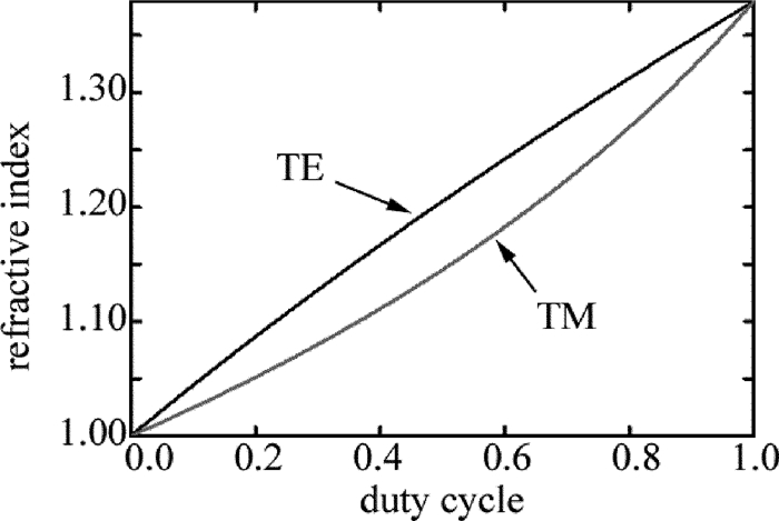
    一些文献中可能会用泰勒公式继续展开(1)式和(2)式,计算周期和波长对等效折射率的影响,但因为周期和波长只有在2阶展开才能体现它们对等效折射率的影响,因此它们其实对等效折射率影响是极其微小,可以忽略[20]。在此不再讨论。图 2是占空比对光栅等效折射率的影响。从图中可知,除了占空比为0和1外,光栅对于TE和TM偏振的等效折射率是不一样的,而且TE偏振的等效折射率比TM的大。

    Figure 2.  Effect of duty cycle on refractive index of TE and TM

    得出光栅等效成薄膜的等效折射率后,可以利用波导理论去计算共振的波长。首先将入射平面波(TE偏振)在光栅层控制光波传播的耦合波方程(3)式和一般平面波导方程(4)式相比:

    式中,Ei(z)是第i级衍射波的振幅,k0=2π/λλ为真空入射光波长,(3)式中最后一项是耦合项。根据平面波导理论可知,β是在平面波导的中所被支持的导波模,可以得出导模共振光栅所支持的导波模即βi=k0(nlsinθ-iλ/Λ)。通过(3)式和(4)式仅推出了光栅所支持的TE偏振的导波模,若要使所支持的导波模存在,则必须是导模共振光栅波导结构的等效折射率neff=βi/k0满足(5)式,同时也可以得出光栅的TE和TM对应的平面波导本征方程(6)式和(7)式。

    式中,${k_i} = {({n_w}^2{k_0}^2- {\beta _i}^2)^{\frac{1}{2}}}$, ${\gamma _i} = {({\beta _i}^2 - {n_{{\rm{eff}}, {\rm{T}}{{\rm{E}}_1}}}^2{k_0}^2)^{\frac{1}{2}}}$, ${\delta _i} = {({\beta _i}^2 - {n_{\rm{s}}}^2{k_0}^2)^{\frac{1}{2}}}$。根据(6)式和(7)式可以得出采用图 1中的导模共振光栅波导结构实现共振的位置,如图 3所示。图中的每一个点即光栅所支持的导波模也是光栅波导结构所激发的导波模。图 3表示的是在光栅周期Λ=500nm、占空比为0.5、厚度h=λ/(4neff),想要激发0阶~2阶模波导层所需的厚度和共振波长的关系。对于TE偏振,若要在波长Λ=850nm处实现共振,0阶导波模(m=0)波导层厚度应为dw=217nm,而1阶模(m=1)和2阶模(m=2)对应的波导层厚度dw分别为644nm和1070nm;对于TM偏振,若要在波长Λ=850nm处实现共振,0阶导波模(m=0)波导层厚度应为dw=310nm,而1阶模(m=1)和2阶模(m=2)对应的波导厚度dw分别为737nm和1160nm。

    Figure 3.  Relationship between dw of TE, dw of TM and λ/Λ

    随后利用严格耦合波法验证由(6)式和(7)式计算得来的波导层厚度能否使0阶模~2阶模均在波长850nm处实现导模共振,计算结果如图 4所示(以TE偏振为例)。从图 4中可以看出,在TE偏振下波导层厚度分别为217nm,644nm,1070nm时,采用图 1结构的导模共振光栅均在波长λ=850nm处实现了共振。

    Figure 4.  Guide mode resonance of 0 order~2nd order modes with wave guide layer thickness of 217nm, 644nm, 1070nm, respectively

2.   器件参量对共振波长和线宽的影响
  • 前面通过波导理论计算了在光栅占空比为0.5、周期为500nm、厚度h=λ/(4neff)时,导模共振光栅若想让0阶模~2阶模均在850mm处出现共振峰,在TE偏振下波导层厚度应为217nm,644nm,1070nm;在TM偏振下波导层厚度应为310nm,737nm,1160nm。为了能够保证单模传输,波导层厚度dw应满足的条件是:217nm≤dw < 310nm,所以为了保持单模,后面若波导层厚度变化,范围均是在217nm~310nm之间,若不变化则设定为217nm,即均是在TE偏振下。

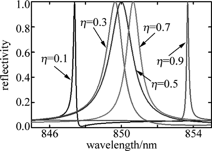
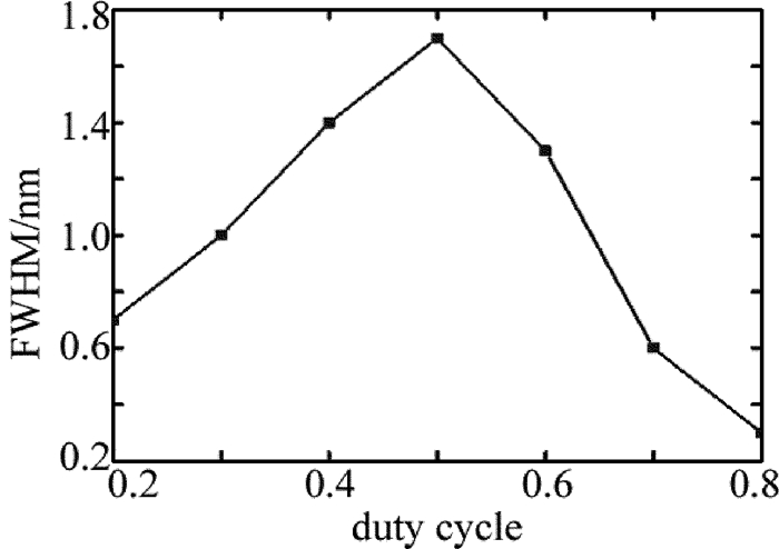
  • 图 5是共振波长随占空比的变化情况。随着占空比的增加,其共振波长也随之增加,这是因为当占空比变化后,通过图 2可得其等效薄膜的折射率也会随之变化,这就使整个波导的等效折射率发生变化,从而导致共振位置发生改变。另外观察发现, 当占空比在0~0.5之间时,反射共振线宽是随着占空比的增大而增大,当占空比在0.5~1之间时, 反射共振线半峰全宽(full width of half maximum, FWHM)随着占空比的增大而减小,如图 6所示。当占空比为0.5时,线宽最大可以达到1.7nm,这是因为此时可以使(3)式中的耦合项sin(πη)/(πη)达到最大; 而当占空比为0或者1时,光栅就不再是真正意义上的光栅,则(3)式就无法适用。

    Figure 5.  Influence of duty cycle on resonance wavelength

    Figure 6.  Influence of duty cycle on resonance line width FWHM

  • 由等效介质理论可知, 周期的变化对光栅的等效折射率几乎没有影响,因此当周期变化的时候不会对图 1的导模共振光栅的有效折射率产生影响。但是在图 3(TE偏振)中,当波导层厚度dw=217nm,横坐标λ/Λ对应的是1.7,故此当周期为500nm时,其对应的共振波长为850nm,而如果周期发生变化,则dw=217nm对应的共振波长就不是850nm。由此可以得出,当周期变化时,导模共振光栅的共振峰对应的波长会发生移动,随着周期的增大,共振波长就向右移动,如图 7所示。从图 7中也可以看见,虽然周期变化共振峰发生迁移,但是不同周期对应的共振线宽是不变化,均是1.7nm(占空比都是0.5)。这是由于周期对(3)式中耦合项没有影响,所以不同周期、相同占空比下,共振线宽是相同的。

    Figure 7.  Influence of period on resonance wavelength

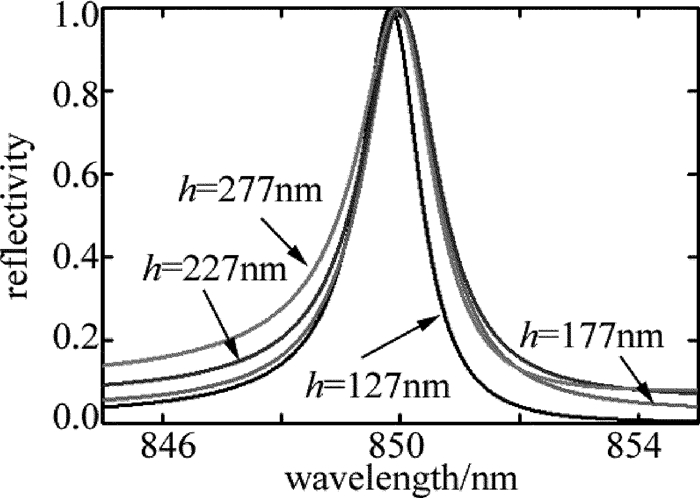
  • 众所周知, 一种材料的折射率仅取决于材料的本质属性而非由其厚度体积所决定,故此类同于光栅的等效折射率其亦非由光栅厚度决定。另外, 从TE和TM平面波导的本征方程以及(3)式中可以得出光栅厚度并不影响共振波长和线宽。图 8显示的是在光栅占空比0.5、周期500nm、波导层厚度217nm时不同光栅厚度对共振波长和线宽的影响。可以发现, 光栅厚度从127nm变化到277nm,导模共振光栅的共振波长和线宽几乎没有发生变化。

    Figure 8.  Influence of thickness on resonance wavelength

  • 入射角也是会改变共振波长。当入射角是0°时, 共振波长是在850nm处,但是当入射角不是0°即入射光不是垂直入射而是斜入射时,则共振波长不再是850nm, 而是会出现两个共振峰,如图 9所示。当入射角是2°时,两个共振峰分别是838nm和865nm;当入射角增大到4°时,两个共振峰分别在820nm和880nm处。通过2°和4°的不同入射角的共振峰对比可以发现, 随着入射角增大,两个共振峰距离也会增大。当入射光是斜入射时,之所以会出现共振峰的分离从而出现两个共振峰,是由于在垂直入射下光栅的±1级倏逝波的导波模是重合的,但是当入射角不为0°时,±1级倏逝波的导波模不再重合,它们会各自拥有对应的导波模,从而会出现图 9中的两个共振峰。

    Figure 9.  Influence of input angle on resonance wavelength

    而对于入射角对共振反射波线宽的影响,同样可以根据(3)式中的耦合项,显然该耦合项中没有关于入射角的参量,由此可知,对于入射角其实并不能影响共振线宽。

  • 图 10所示的是波导层厚度对共振波长的影响。当波导层厚度为217nm时,共振波长为850nm; 而当波导层厚度增加到251nm时,共振峰就落在866nm处。由此可以发现, 波导层厚度对共振波长的影响非常的显著,之所以会有这样的影响,同样可以从图 3(TE偏振)得出,由于波导层厚度的增加,其纵坐标会上移,则所对应的横坐标λ/Λ就不再是1.7,而是大于1.7,由于周期是不变的(依然是500nm),故而其共振波长会增加, 并且增加得非常明显。

    Figure 10.  Influence of wave-guide layer thickness on resonance wavelength

    从图中可以看见, 无论波导层厚度怎么变化,其共振线宽始终没有变化, 一直是1.7nm(占空比0.5),这是因为由(3)式中的耦合项可以看见, 仅有占空比η对其有影响,而周期、波导层厚度、光栅厚度等均没有出现在(3)式的耦合项中。

3.   结论
  • 通过等效介质理论和波导理论,设计出了在850nm处具有导模共振现象的光栅结构,并在严格耦合波法上得到验证。同时也利用严格耦合波法分析了光栅参量(占空比、周期、厚度)、入射角以及波导层厚度对共振波长和线宽的影响。通过计算可知,光栅占空比对共振线宽和波长均有影响,随着占空比的增大,共振波长增大,但是共振线宽只有在占空比为0.5时才是最大, 采用图 1中的结构可以达到1.7nm;光栅周期仅对共振线宽有影响, 随着周期的增大,共振波长也会增大而线宽不变;光栅厚度对共振线宽和周期均没有影响;当入射光不是垂直入射即入射角不为0°时,会出现两个共振峰,而且随着入射角的增大两个共振峰相距越大;波导层厚度和光栅周期一样对共振波长影响非常显著,但是其对共振线宽没有影响。通过850nm导模共振光栅的设计以及计算其参量对共振线宽和波长的影响,可以帮助对导模共振光栅的理解以及更好地对工艺制作进行指导。

Reference (20)

Catalog

    /

    DownLoad:  Full-Size Img  PowerPoint
    Return
    Return