Advanced Search

ISSN1001-3806 CN51-1125/TN Map

Volume 42 Issue 5
Sep.  2018
Article Contents
Turn off MathJax

Citation:

Study on phase difference of all-optical logic XOR gates

  • Corresponding author: WANG Hailong, phyhlwang71@126.com
  • Received Date: 2017-10-30
    Accepted Date: 2017-12-18
  • In order to optimize the phase difference of the all-optical logic gates, the phase difference of all-optical logic exclusive OR (XOR) gates was studied. Firstly, the refined sectionalized model was used simulate the dynamic process of quantum-dot semiconductor optical amplifier (QD-SOA). Secondly, the Newton method and the four-order Runge-Kutta method were used to solve the three-level transition rate equations and the light field transfer equations. Finally, an all-optical logic XOR gate based on quantum-dot semiconductor optical amplifier Mach-Zehnder interferometer (QD-SOA-MZI) was implemented. The influence of the length of the active regions, the maximum modal gain, input pump power and input pump pulse width on phase difference of probe signal through two arms of the interferometer was studied in detail. Moreover, the relationship between phase difference of the probe signal and output optical power was also discussed. The results show that, with the increase of the length of the active regions, the maximum modal gain and input pump power can lead to improve phase difference of probe signal through two arms of the interferometer. With the increase of input pump pulse width, phase difference of probe signal through two arms of the interferometer increases at first and then decreases. When the length of the active region is 2.0mm, the maximum modal gain is 3000m-1, the input pump power is 5dBm, and input pump pulse width is 1.0ps, the maximum phase difference of probe signal through two arms of the interferometer increases 0.3277π. Output optical power also can be improved by the increase of probe signal phase difference. Phase difference of the detected light can be increased by optimizing the parameters. Output light power increases with the increase of the phase difference of the probe. This study provides a reference for improving the quality of conversion signals.
  • 加载中
  • [1]

    CHEN D, WANG R, PU T, et al. A novel thresholder based on XGM effect in a DFB laser combined with external optical filtering[J]. IEEE Photonics Journal, 2016, 8(1): 1-7.
    [2]

    SHI Sh Sh, WANG H L, GONG Q, et al. Refined sectionalized method of QD-SOA[J]. Optik-International Journal for Light and Electron Optics, 2014, 125(1): 504-507.
    [3]

    SINGH P, TRIPATHI D K, JAISWAL S, et al. Designs of all-optical buffer and OR gate using SOA-MZI[J]. Optical and Quantum Electronics, 2014, 46(11): 1435-1444. doi: 10.1007/s11082-013-9856-0
    [4]

    ZAJNULINA M, LINGNAU B, LVDGE K. Four-wave mixing in quantum-dot semiconductor optical amplifiers: A detailed analysis of the nonlinear effects[J]. IEEE Journal of Selected Topics in Quantum Electronics, 2017, 23(6): 1-12.
    [5]

    KOTB A. Simulation of high quality factor all-optical logic gates based on quantum-dot semiconductor optical amplifier at 1Tb/s[J]. Optik-International Journal for Light and Electron Optics, 2016, 127(1): 320-325. doi: 10.1016/j.ijleo.2015.10.093
    [6]

    CUI L L, WANG H L, LI W, et al. Study on gain recovery time of wavelength conversion based on single-port-coupled QD-SOA[J]. Laser Technology, 2016, 40(5): 742-745(in Chinese).
    [7]

    AMOR L. All-optical networks: Security issues analysis[J]. Journal of Optical Communications and Networking, 2015, 7(3): 136-145. doi: 10.1364/JOCN.7.000136
    [8]

    TAN H N, INOUE T, SOLIS-TRAPALA K, et al. On the cascadability of all-optical wavelength converter for high-order QAM formats[J]. Journal of Lightwave Technology, 2016, 34(13): 3194-3205. doi: 10.1109/JLT.2016.2545246
    [9]

    MATAUURA M, OHTA H, SEKI R. Experimental investigation of chirp properties induced by signal amplification in quantum-dot semiconductor optical amplifiers[J]. Optics Letters, 2015, 40(6): 914-917. doi: 10.1364/OL.40.000914
    [10]

    ALIMOHAMMADI F, YADIPOUR R, ABBASIAN K, et al. THz-assisted instantaneous gain switching in quantum dot semiconductor optical amplifiers[J]. IEEE Photonics Technology Letters, 2015, 27(3): 288-291. doi: 10.1109/LPT.2014.2369514
    [11]

    EYAL O, WILLINGER A, BANYOUDEH S, et al. Static and dynamic characteristics of an InAs/InP quantum-dot optical amplifier operating at high temperatures[J]. Optics Express, 2017, 25(22): 27262-27269. doi: 10.1364/OE.25.027262
    [12]

    YANG W H, WANG H L, WANG Zh X, et al.Wavelength conversion efficiency of quantum dot semiconductor optical amplifier[J].Acta Optica Sinica, 2017, 37(4):0406005(in Chinese). doi: 10.3788/AOS
    [13]

    CHEN T T, WANG H L, LIU S, et al. Theoretical study on chirp of wavelength conversion based on QD-SOA[J]. Laser Technology, 2016, 40(2): 292-295(in Chinese).
    [14]

    NURMOHAMMADI T, ABBASIAN K, AS'ADI M J, et al. Design of an ultrafast all-optical NOR logic gate based on Mach-Zehnder interferometer using quantum-dot SOA[J]. Optik-International Journal for Light and Electron Optics, 2014, 125(15): 4023-4029. doi: 10.1016/j.ijleo.2014.01.119
    [15]

    TALEB H, ABEDI K. Design of a low-power all-optical NOR gate using photonic crystal quantum-dot semiconductor optical amplifiers[J]. Optics Letters, 2014, 39(21): 6237-6240. doi: 10.1364/OL.39.006237
    [16]

    SINGH P, TRIPATHI D K, DIXIT H K. Designs of all-optical NOR gates using SOA based MZI[J]. Optik-International Journal for Light and Electron Optics, 2014, 125(16): 4437-4440. doi: 10.1016/j.ijleo.2014.02.032
    [17]

    GAYEN D K, CHATTOPADHYAY T. Designing of optimized all-optical half adder circuit using single quantum-dot semiconductor optical amplifier assisted Mach-Zehnder interferometer[J]. Journal of Lightwave Technology, 2013, 31(12): 2029-2035. doi: 10.1109/JLT.2013.2263251
    [18]

    GAYEN D K, CHATTOPADHYAY T. Simultaneous all-optical basic arithmetic operations using QD-SOA-assisted Mach-Zehnder interferometer[J]. Journal of Computational Electronics, 2016, 15(3): 982-992.
    [19]

    KOTB A, ALAMER F A. Dispersion on all-optical logic XOR gate using semiconductor optical amplifier[J]. Optical and Quantum Electronics, 2016, 48(6): 1-10.
    [20]

    HU Z, XIANG B, XING Y. Optical gain depending on both size fluctuations of quantum dots and temperature in InGaAs/GaAs QD-SOA[J]. IEEE Transactions on Electron Devices, 2017, 64(9): 3683-3689. doi: 10.1109/TED.2017.2722383
  • 加载中
通讯作者: 陈斌, bchen63@163.com
  • 1. 

    沈阳化工大学材料科学与工程学院 沈阳 110142

  1. 本站搜索
  2. 百度学术搜索
  3. 万方数据库搜索
  4. CNKI搜索

Figures(13) / Tables(2)

Article views(4845) PDF downloads(168) Cited by()

Proportional views

Study on phase difference of all-optical logic XOR gates

    Corresponding author: WANG Hailong, phyhlwang71@126.com
  • 1. Shandong Provincial Key Laboratory of Laser Polarization and Information Technology, Department of Physics, Qufu Normal University, Qufu 273165, China
  • 2. State Key Laboratory of Functional Materials for Informatics, Shanghai Institute of Microsystem and Information Technology, Chinese Academy of Sciences, Shanghai 200050, China

Abstract: In order to optimize the phase difference of the all-optical logic gates, the phase difference of all-optical logic exclusive OR (XOR) gates was studied. Firstly, the refined sectionalized model was used simulate the dynamic process of quantum-dot semiconductor optical amplifier (QD-SOA). Secondly, the Newton method and the four-order Runge-Kutta method were used to solve the three-level transition rate equations and the light field transfer equations. Finally, an all-optical logic XOR gate based on quantum-dot semiconductor optical amplifier Mach-Zehnder interferometer (QD-SOA-MZI) was implemented. The influence of the length of the active regions, the maximum modal gain, input pump power and input pump pulse width on phase difference of probe signal through two arms of the interferometer was studied in detail. Moreover, the relationship between phase difference of the probe signal and output optical power was also discussed. The results show that, with the increase of the length of the active regions, the maximum modal gain and input pump power can lead to improve phase difference of probe signal through two arms of the interferometer. With the increase of input pump pulse width, phase difference of probe signal through two arms of the interferometer increases at first and then decreases. When the length of the active region is 2.0mm, the maximum modal gain is 3000m-1, the input pump power is 5dBm, and input pump pulse width is 1.0ps, the maximum phase difference of probe signal through two arms of the interferometer increases 0.3277π. Output optical power also can be improved by the increase of probe signal phase difference. Phase difference of the detected light can be increased by optimizing the parameters. Output light power increases with the increase of the phase difference of the probe. This study provides a reference for improving the quality of conversion signals.

引言
  • 随着信息时代的不断发展,人们对信息传输速度、容量以及通信质量的要求不断提高,而传统的光网络并不能满足这一需求。全光网络[1]中从源节点到目的节点传输的数据均以光的形式进行,不存在传统光网络中光-电-光[2]的转换过程,使得各个节点间的传输过程都发生在光域之中。在全光网络中,由于通过波长来选择路由,不受传输光信号调制方式和传输速率的限制,所以提高了传输的网络透明性。同时全光网络[3]还具有兼容性较好、高集成性、重组灵活、结构简单以及维护费用低等优点,从而成为研究的热点。

    在全光网络中,全光逻辑处理技术在光通信网络节点、全光传输和光计算等过程中具有重要的作用,是实现信息交换的核心。由于引入全光逻辑器件[4],克服了电子技术本身存在的“电子瓶颈”[5],同时也满足了扩大光网络的工作容量、有效降低信号噪声以及提高光网络传输速率的需求。目前已经出现了不少全光逻辑异或门的实现方案,例如半导体光放大器-Sagnac光纤干涉仪[6]、超快线性干涉仪(ultrafast nonlinear interferometer, UNI)[7]等。这些方法利用光纤的非线性效应[8]实现异或运算,具有数据处理速度快的优点,但这也使异或门结构变得复杂,难以集成[9-10]

    由于量子点半导体光放大器(quantum-dot semiconductor optical amplifier, QD-SOA)相比于其它类型的光放大器具有更高的温度稳定性、噪声指数较低、饱和功率高以及超快的增益恢复特性等优点[11],同时马赫-曾德尔干涉仪(Mach-Zehnder interferometer, MZI)具有结构紧凑、工作稳定等优点,所以基于量子点半导体光放大器马赫-曾德尔干涉仪(quantum-dot semiconductor optical amplifier Mach-Zehnder interferometer, QD-SOA-MZI)结构的全光逻辑异或门相比于其它方案的逻辑异或门而言, 具有结构更加简单、可重复性高、功耗低以及延时短等优点,并且非常适用于复杂的逻辑电路。之前对基于QD-SOA-MZI的全光逻辑异或门转换光的转换效率进行了讨论[12]。本文中在实现基于QD-SOA-MZI结构的全光逻辑异或门的基础上,进一步详细分析了通过干涉仪两臂后探测光的相位差特性,同时讨论了相位差与输出光功率关系。

1.   基本原理
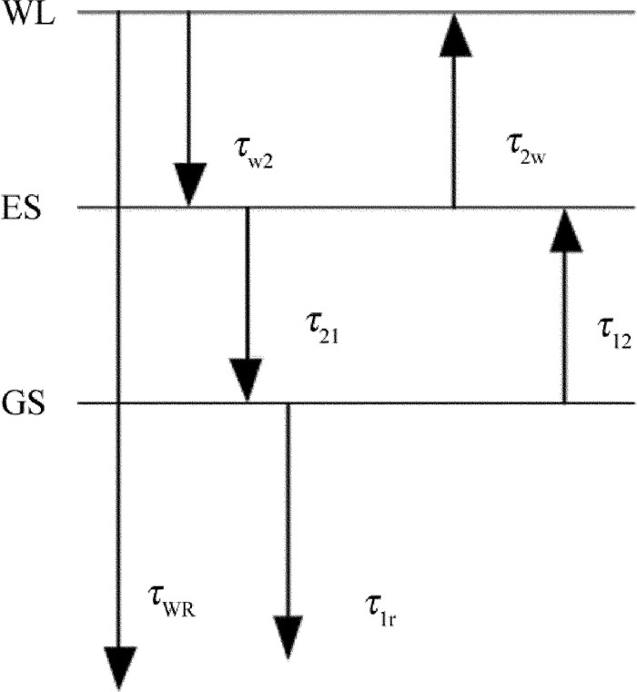
  • 图 1所示为浸润层(wetting layer, WL)、激发态(excited state, ES)和基态(ground state, GS)所构成的QD-SOA的三能级结构[13]

    Figure 1.  Energy level structure of QD-SOA

    其中WL的载流子浓度变化以及电子在ES和GS的占有几率变化用三能级跃迁速率方程表示为[14]

    式中,NWL表示浸润层中的载流子浓度; Nq表示表面量子点密度; Lw, σ分别表示有源区厚度以及有源区横截面积; J, e分别表示注入电流密度和电子电量; h表示电子在激发态中的占有几率,f表示电子在基态中的占有几率; τWR, τ1r分别表示电子在浸润层中的自发辐射时间以及电子在量子点中的自发辐射时间; τ2w表示电子从激发态到浸润层的跃迁时间,τ21表示电子从激发态到基态的跃迁时间,电子从浸润层到激发态的弛豫时间为τw2,电子从基态到激发态的跃迁时间为τ12; h1ωi表示光子能量,ωi为光频率; h1为电子在激发态中占有几率的初始值; gi表示第i段的模式增益; P为输出光功率。

    假设QD-SOA的端面反射率为0,而且忽略放大自发辐射(amplified spontaneous emission, ASE)噪声,即QD-SOA处于理想状态时,输入光在QD-SOA中传输的光场方程表示为[15]

    式中, 光场限制因子为Γz表示光场传输方向,E+, E分别表示输入光沿z方向(+z)以及沿z的相反方向(-z)传播的光场强度,ηα分别表示线宽增强因子和波导损耗系数, g为模式增益,可简单表示为g=gmax(2f-1), 其中gmax是最大模式增益。

    用(6)式和(7)式来表示光场传输方程(4)式和(5)式的边界条件:

    式中, Ein是初始输入光场强度,r1为前端面反射系数,r2为后端面反射系数。

    沿着光的传输方向,探测光受到抽运光的调制以及自身相位的调制,从而导致探测光相位发生改变,由下式来表示探测光的相位变化[16]

    对(8)式沿着QD-SOA有源区+L方向积分,得到(9)式,即相位随时间的变化可表示为[17]

    式中,g(z, t)是引入转换坐标系后的模式增益。

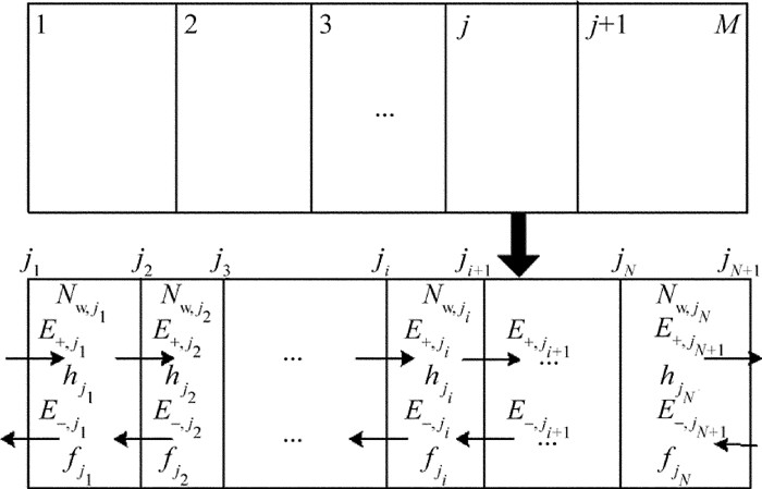
    图 2所示为QD-SOA细化分段模型。首先将QD-SOA分成等长的M小段,当M足够大时,将各段中的载流子近似看作是均匀的,并将第j段内的载流子浓度记作Nj(t)。为了对每一段有源区内的载流子变化情况有更精确的描述,将第j段再细化分成N段,此时将每一小段记作ΔL=L/(M×N)。

    Figure 2.  The refined sectionalized model of QD-SOA

  • 利用MZI结构实现全光逻辑异或门(exclusive OR, XOR)方案,如图 3所示。在干涉仪的上下两臂分别放置两个完全相同的QD-SOA,波长为λ1的探测光通过分波器C1分解成两束完全相同的光,波长为λ2的信号分别和两束探测光经过耦合器C2, C3输入到干涉仪的QD-SOA1和QD-SOA2中。由于信号的输入功率大于QD-SOA的最大线性输入功率,使得信号光在经过QD-SOA时会对探测光进行相位调制。通过干涉仪两臂后的探测光将在耦合器C4中发生干涉,实现全光逻辑异或门。

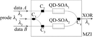
    Figure 3.  Structure diagram for all-optical logic XOR gate based on QD-SOA-MZI

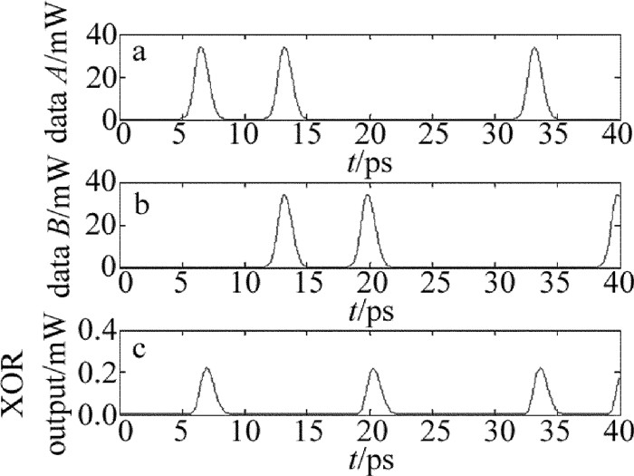
    当data A, data B都为“0”时,由于不存在输入光信号,所以输出信号不存在,即输出信号表示为逻辑“0”;当data A, data B不同时,例如data A为“1”,data B为“0”时,经过MZI上臂QD-SOA1的探测光受到data A的调制,而经过MZI下臂QD-SOA2的探测光没有受到调制,此时通过上下两臂的探测光相位差为π,因此二者发生干涉相消后输出信号表示为逻辑“1”;当data A, data B都为“1”时,经过QD-SOA1和QD-SOA2的探测光均会受到信号光的调制,此时相位差为0,因此二者发生干涉相长后输出信号表示为逻辑“0”,从而实现了逻辑异或运算,并且输出光实现了波长转换。将输出光功率表示为[18]

    式中, Pprobe是输入探测光信号的功率,G1(t), G2(t)是探测光分别通过干涉仪QD-SOA1、QD-SOA2后的增益,ϕ1(t), ϕ2(t)分别是经过MZI上下两臂QD-SOA的探测光受到调制后的相位,k1, k2表示耦合器的耦合系数,取值为k1=k2=0.5。表 1所示为全光逻辑异或运算的真值表[19]

    A B C(AB=C)
    1 1 0
    1 0 1
    0 1 1
    0 0 0

    Table 1.  Truth table of XOR gate

2.   数值模拟
  • 为了研究基于QD-SOA-MZI结构的全光异或逻辑门的相位差特性,利用牛顿法和4阶龙格-库塔法求解(1)式~(5)式,所取参量如表 2所示[20]

    parameter value
    optical confinement factor Γ 0.5
    absorption coefficient of the material αint 300m-1
    thickness of wetting layer Lw 0.2μm
    surface density of QD Nq 5×10¹⁴m-2
    spontaneous radiative lifetime in QD τ1r 0.4ns
    spontaneous radiative lifetime in WL τWR 2ns
    electron escape time from GS to ES τ12 1.2ps
    electron relaxation time from ES to GS τ21 0.16ps
    electron escape time from ES to WL τ2w 1ns
    electron relaxation time from WL to ES τw2 3ps

    Table 2.  Parameters for numerical calculation

    在对QD-SOA-MZI逻辑异或门进行数值模拟时,假设探测光波长λ1=1550nm,输入data A和data B是脉冲宽度为0.4ps的1阶高斯脉冲信号,data A和data B的波长λ2=1500nm,取输入的光信号峰值功率Pp=-5dBm,采用细化分段模型对QD-SOA进行建模,取分段数N=100。图 4所示为数值模拟实现的全光逻辑异或运算结果。

    Figure 4.  Calculation results of all-optical logic XOR gate based on QD-SOA-MZI

    当探测光通过干涉仪的上下两臂时,由于QD-SOA1和QD-SOA2内载流子浓度的改变影响了折射率,导致探测光产生相位变化,经过光的干涉作用,这种相位变化会转变成输出光功率的变化。将通过QD-SOA1和QD-SOA2后输出的探测光相位之差定义为相位差,表示为:

    图 5所示为通过MZI两臂的探测光相位随时间的变化。其中, 图 5a图 5b分别为干涉仪两臂输出的探测光相位,图 5c为经过调制后探测光的相位差。下面将分别讨论有源区长度、最大模式增益、抽运光功率、以及输入抽运光脉冲宽度对全光逻辑异或门相位差的影响以及随着相位差的改变输出光功率的变化。

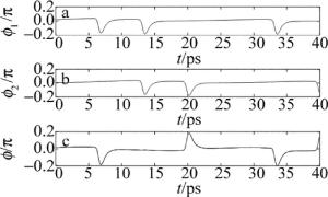
    Figure 5.  Phase of probe signals through two arms of MZI
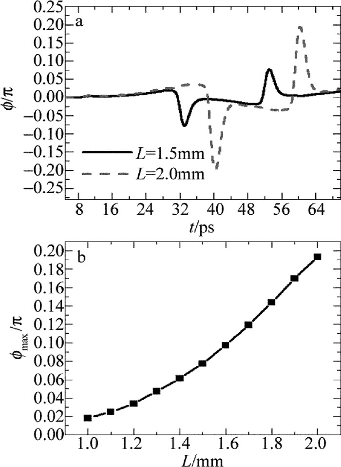
  • 图 6a可知,随着有源区长度的增加,光增益增大,载流子发生受激辐射的概率增加,导致QD-SOA中载流子消耗加快,此时有源区的折射率提高,使得连续光分别通过MZI中QD-SOA1和QD-SOA2后产生的相位差增大。图 6b更清楚地显示出随着有源区长度增加,探测光的相位差不断增大。当有源区长度为1.5mm时,探测光的最大相位差为0.0774π;当有源区长度为2.0mm时,探测光的最大相位差为0.1932π。但是当QD-SOA的有源区长度太长时,会导致自发辐射噪声增大,此时信号光的输出波形会受到影响。

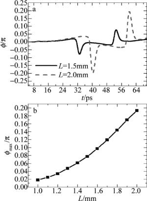
    Figure 6.  a—relationship between phase difference and time with different lengths b—relationship between phase difference and length of the active regions

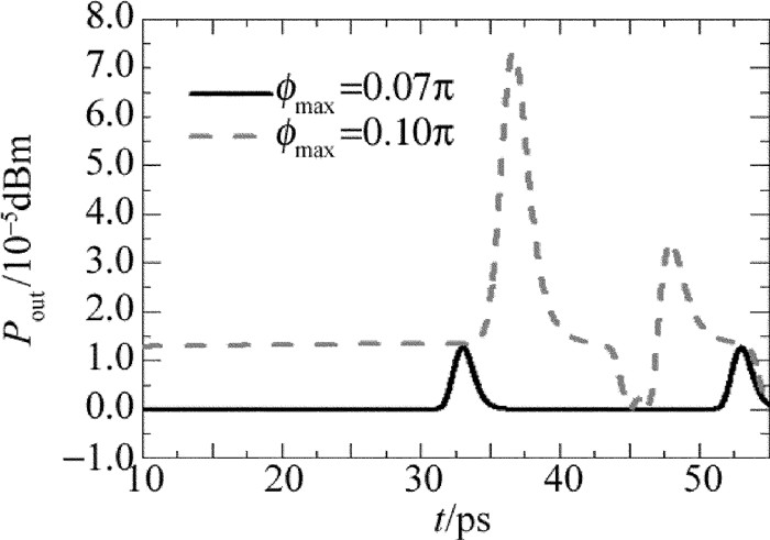
    图 7中给出了探测光最大相位差分别为0.07π, 0.10π时的输出波形图像。当探测光的最大相位差为0.07π时,输出光峰值功率为1.2699×10⁻⁵dBm;当探测光的最大相位差为0.10π时,输出光峰值功率为7.7471×10⁻⁵dBm。容易看出,当相位差较大时,输出光功率较大。这是由于有源区长度不断增加使得探测光相位差不断增大,经过光的相互干涉,相位差的改变进而转化为输出光功率的变化。因此随着相位差的增加,输出光功率不断增大。

    Figure 7.  Output optical power varying with time at different phase differences

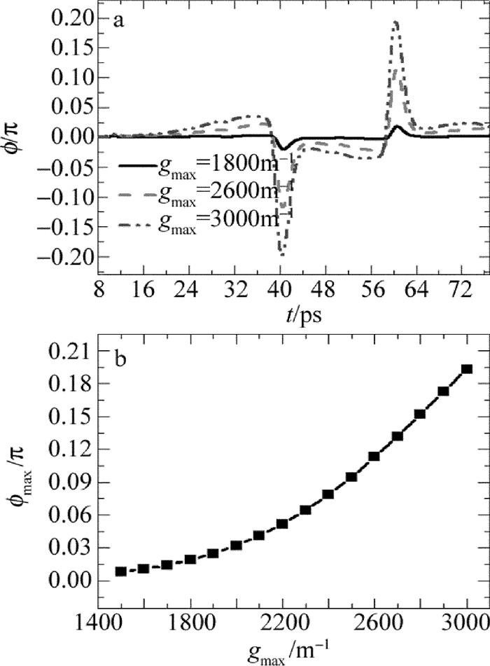
  • 图 8a为最大模式增益gmax取1800m-1, 2600m-1, 3000m-1时相位差随时间的变化规律。可以看出,最大模式增益不同, 得到的随时间变化的相位差的极值不同; 最大模式增益增大,探测光相位差不断增大。图 8b更清楚地显示了gmax对探测光相位差的影响。当gmax=1800m-1时,探测光的最大相位差为0.0192π;当gmax=2600m-1时,探测光的最大相位差为0.1138π;当gmax=3000m-1时,探测光的最大相位差为0.1933π。这是因为增大gmax,光增益随之增大,QD-SOA有源区内载流子与输入光发生受激辐射的概率增大,而且速率也会增加,导致载流子快速消耗,然而消耗速率加快使得有源区内的载流子得不到及时的补充,所以相位差增大。

    Figure 8.  Relationship between maximum modal gain and phase difference
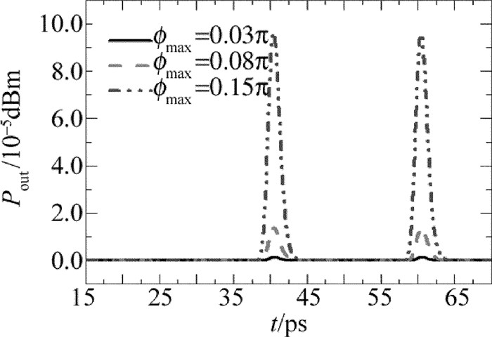
    图 9所示,当探测光的最大相位差为0.03π时,输出光峰值功率为1.3320×10⁻⁶dBm;当探测光的最大相位差为0.08π时,输出光峰值功率为1.3718×10⁻⁵dBm;当探测光的最大相位差为0.15π时,输出光峰值功率为9.6443×10⁻⁵dBm。这是由于最大模式增益增大使得探测光的相位差增大,经过光的干涉作用,这种相位差的变化转变为输出光功率的变化,从而使得输出光功率随着相位差的增大而增大。

    Figure 9.  Relationship between output optical power and time with different phase differences: 0.03π, 0.08π, 0.15π
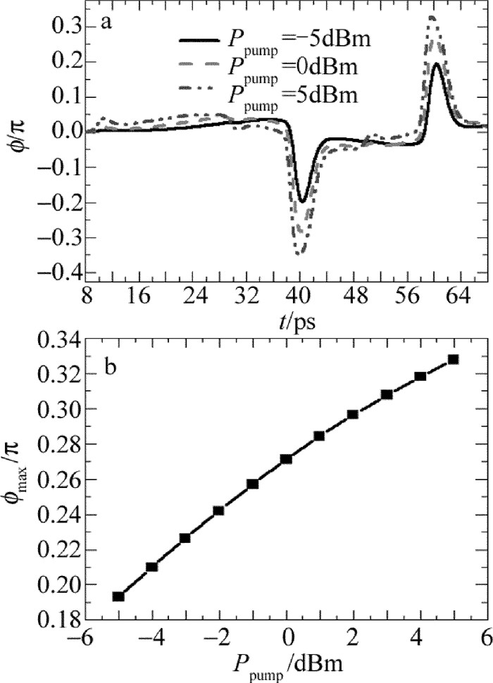
  • 图 10a所示,当抽运光功率不断增大时,由于QD-SOA有源区中迅速降低的载流子浓度引起有效折射率快速变化,导致连续光通过干涉仪的QD-SOA1和QD-SOA2调制后产生的相位差增大。图 10b中进一步说明了探测光相位差与抽运光功率的关系。当抽运光功率为-5dBm时,探测光的最大相位差为0.1933π;当抽运光功率为0dBm时,探测光的最大相位差为0.2711π;当抽运光功率为5dBm时,探测光的最大相位差为0.3277π。因此,随着抽运光功率增加,探测光相位差增大。

    Figure 10.  a—relationship between phase difference and time with different pump power b—relationship between phase difference and pump power

    图 11所示为探测光最大相位差分别是0.20π, 0.25π, 0.30π时的输出波形图像。由图可知,输出光功率随着探测光相位差的增大而增大。当探测光的最大相位差为0.20π时,输出光峰值功率为2.6882×10⁻⁴dBm;当探测光最大相位差为0.25π时,输出光峰值功率为4.4908×10⁻⁴dBm;当探测光最大相位差为0.30π时,输出光峰值功率为7.3254×10⁻⁴dBm。这是因为随着抽运光功率不断增大,探测光相位差不断增加,由于光的干涉作用,相位差的变化进而引起输出光功率的变化。所以当探测光相位差增大时,输出光功率不断增大。

    Figure 11.  Relationship between output optical power and time with different phase differences: 0.20π, 0.25π, 0.30π

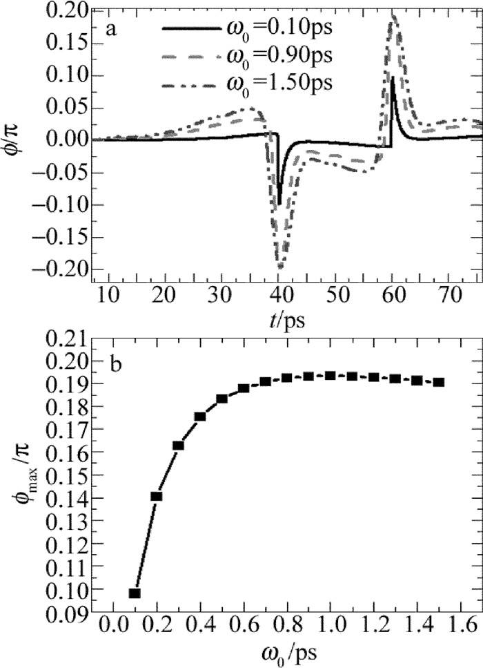
  • 图 12a显示了脉冲宽度为0.10ps, 0.90ps, 1.50ps时测得的相位差随时间的变化规律。由图可知,脉冲宽度不同时测得的随时间变化的相位差极值不同。这是由于保持输入脉冲的功率不变,增加脉冲宽度,使得载流子更早发生受激辐射,而且载流子消耗速率加快,导致相位差快速增大;但是当脉冲宽度增大到一定程度时,有源区内载流子浓度变化逐渐减缓,使得相位差缓慢减小。图 12b更清晰地显示出探测光相位差随脉冲宽度的变化。可知当脉冲宽度为0.10ps时,探测光的最大相位差为0.0978π;当脉冲宽度为0.90ps时,探测光的最大相位差为0.1930π;当脉冲宽度为1.50ps时,探测光的最大相位差为0.1904π。由此可见,当脉冲宽度增大时,探测光相位差先增大之后趋于平缓再不断减小。

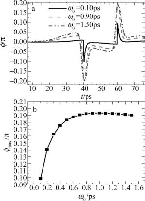
    Figure 12.  a—relationship between phase different and time b—relationship between with phase different and pulse width

    图 13所示,当探测光的最大相位差为0.14π时,输出光峰值功率为8.4209×10⁻⁵dBm;当探测光的最大相位差为0.19π时,输出光峰值功率为2.1935×10⁻⁴dBm。可见随着相位差的增大,输出光功率增大。这是由于增大脉冲宽度,探测光相位差会发生改变,经过光的干涉作用,这种相位差的变化转变为输出光功率的变化,从而使得输出光功率随着相位差的增大而增大。

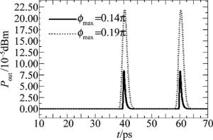
    Figure 13.  Relationship between output optical power and time at different phase differences

3.   结论
  • 基于QD-SOA的交叉相位调制效应,利用MZI结构,实现了基于QD-SOA-MZI的全光逻辑异或门功能。分析了通过干涉仪上下两臂探测光的相位差特性以及相位差对输出光功率的影响。数值模拟结果表明:随着有源区长度、最大模式增益以及输入抽运光功率的增大,导致通过干涉仪两臂的探测光经过调制后产生的相位差增大;当抽运光脉冲宽度增大时,探测光相位差先增大而后趋于平缓之后不断减小。另外进一步对探测光的相位差与输出光功率之间的关系进行了模拟。模拟结果表明,通过优化参量增大探测光的相位差,可以使输出光功率增大。

Reference (20)

Catalog

    /

    DownLoad:  Full-Size Img  PowerPoint
    Return
    Return