Advanced Search

ISSN1001-3806 CN51-1125/TN Map

Volume 42 Issue 5
Sep.  2018
Article Contents
Turn off MathJax

Citation:

Palladium free activation and electroless nickel plating on ceramic surface

  • Corresponding author: ZHONG Liang, 758358099@qq.com
  • Received Date: 2017-12-05
    Accepted Date: 2018-01-17
  • In order to realize palladium free electroless nickel plating on the surface of the ceramic matrix, the mixed solution of 10g/L NiSO4·6H2O and 45g/L NaH2PO2 was used as activation solution and was coated on the surface of the matrix. The substrate was activated by laser scanning, and then electroless nickel was carried out. The effect of laser power, spot diameter and scanning rate on coating coverage was studied. The microstructure of coarsening, activation and plating was observed by a scanning electron microscope. The composition analysis of the substrate surface after activation and plating was analyzed. The adhesion, electrical conductivity and solderability of the coating were detected. The results show that, when laser power is 3W, the diameter of the spot is 2mm and scanning rate is 5mm/s, a layer of Ni particles with an average diameter of 0.1μm is generated on the substrate surface. The coating coverage is 100%. Micro surface of the coating is smooth and dense and the diameter of the cell is above 10μm. Mass fraction of P in plating layer is 0.0771, with good wear resistance and corrosion resistance for the amorphous structure. The coating has strong adhesion and good weldability. It is good conductor with the resistivity of 7.67×10⁻⁵Ω·cm. With low cost and pollution-free, the process can realize local electroless nickel plating on the surface of ceramic matrix. By controlling the motion of laser, all kinds of fine graphics can be deposited on the surface of the matrix. The process has a certain practical value.
  • 加载中
  • [1]

    YAN X Y. The application of ceramic materials[J]. China Electronic Business:Component Market, 2001(9):48(in Chinese).
    [2]

    KINGERY W D. Introduction to Ceramics[J]. Journal of the Electrochemical Society, 1960, 124(3):152C.
    [3]

    ZENG L K, WANG H. Surface modification technology of ceramic materials[M]. Beijing:Chemical Industry Press, 2006:46-50(in Chinese).
    [4]

    REN Ch Q, XIE F Q. Electronic ceramic electroless plating and application[J]. Electronic Technology, 2003, 24(1):32-35(in Chin-ese).
    [5]

    LI Zh, DAI L, HUANG X B, et al. Effect of activation process on electroless nickel plating[J]. Electroplating & Pollution Control, 2016, 36(6):22-24(in Chinese).
    [6]

    LI R, YU Q L. Electroless Ni-P plating on porcelain ganule and glass substrates[J]. Corrosion & Protection, 2008, 29(11):691-693(in Chinese).
    [7]

    CHENG L, BAO D M, YANG L, et al. Research progress on nickel colloidal activation electroless plating on ceramic surface[J]. Guangzhou Chemical Industry, 2017, 45(15):108-110(in Chinese).
    [8]

    GU X, WANG Zh Ch, LIN Ch J. New developing of pretreatment process for electroless plating of ceramics[J]. Material Protection, 2003, 36(9):1-4(in Chinese).
    [9]

    ZHENG X H, SHAN D D, SONG H, et al. Electroless nickel plating process and properties of alumina ceramics[J]. Surface Technology, 2017, 46(10):126-134(in Chinese).
    [10]

    LI L B, LI D P, ZHANG Sh H, et al. Research on electroless Ni-P alloy plating on ceramics surface[J]. Electroplating & Pollution Control, 2011, 31(3):19-21(in Chinese).
    [11]

    LI B, WEI X W, ZHANG Zh Y, et al. Study on activation technology of electroless nickel plating on nonmetallic materials[J]. Material Protection, 2001, 34(2):17-18(in Chinese).
    [12]

    FU Sh L, LI Y H, WANG B G, et al. Investigation on palladium-free activation nickel electroless plating on glass[J]. Plating & Finishing, 2000, 22(5):10-13(in Chinese).
    [13]

    LIU Z, GAO W. The effect of substrate on the electroless nickel plating of Mg and Mg alloys[J]. Surface & Coatings Technology, 2006, 200(11):3553-3560.
    [14]

    YAN J P, LIN W H, LU L L, et al. Effect of surface roughening on chemical nickel-plating on zirconia precision ceramic[J]. Corrosion & Protection, 2017, 38(4):268-272(in Chinese).
    [15]

    ZHONG X Q, QIN M L, LI H, et al. The technology research of electroless nickel plating on AlN ceramic surface[J]. Vacuum Electronics, 2011(3):14-17(in Chinese).
    [16]

    ZHOU Z X, CHENG H B, XUE L H, et al. The methods of improving and checking adhesion of coating electroless-plated[J]. Mate-rials Review, 2006, 20(2):79-81(in Chinese).
    [17]

    ZHANG F X, ZHONG L, LIAO Y P. Electroless copper plating process for fiber bragg grating and its characteristics[J]. Modern Chemical Industry, 2014, 34(7):96-99(in Chinese).
    [18]

    LI F, LI B. Effect of gold thickness on ENIG PCB solder spread and joint reliability[J]. Electroplating & Finishing, 2015, 34(4):196-200(in Chinese).
    [19]

    GAO C, DAI L, MENG W, et al. Electrochemically promoted electroless nickel-phosphorous plating on titanium substrate[J]. Applied Surface Science, 2017, 392:912-919. doi: 10.1016/j.apsusc.2016.09.127
    [20]

    GAO J Q. A research on the control of phosphorous content in electroless Ni-P coating and the effect on the performances of the coating[J].Electroplating & Pollution Control, 2002, 22(1):1-4(in Ch-inese).
  • 加载中
通讯作者: 陈斌, bchen63@163.com
  • 1. 

    沈阳化工大学材料科学与工程学院 沈阳 110142

  1. 本站搜索
  2. 百度学术搜索
  3. 万方数据库搜索
  4. CNKI搜索

Figures(11) / Tables(1)

Article views(5568) PDF downloads(172) Cited by()

Proportional views

Palladium free activation and electroless nickel plating on ceramic surface

    Corresponding author: ZHONG Liang, 758358099@qq.com
  • College of Science and Engineering, Southwest University of Science and Technology, Mianyang 621000, China

Abstract: In order to realize palladium free electroless nickel plating on the surface of the ceramic matrix, the mixed solution of 10g/L NiSO4·6H2O and 45g/L NaH2PO2 was used as activation solution and was coated on the surface of the matrix. The substrate was activated by laser scanning, and then electroless nickel was carried out. The effect of laser power, spot diameter and scanning rate on coating coverage was studied. The microstructure of coarsening, activation and plating was observed by a scanning electron microscope. The composition analysis of the substrate surface after activation and plating was analyzed. The adhesion, electrical conductivity and solderability of the coating were detected. The results show that, when laser power is 3W, the diameter of the spot is 2mm and scanning rate is 5mm/s, a layer of Ni particles with an average diameter of 0.1μm is generated on the substrate surface. The coating coverage is 100%. Micro surface of the coating is smooth and dense and the diameter of the cell is above 10μm. Mass fraction of P in plating layer is 0.0771, with good wear resistance and corrosion resistance for the amorphous structure. The coating has strong adhesion and good weldability. It is good conductor with the resistivity of 7.67×10⁻⁵Ω·cm. With low cost and pollution-free, the process can realize local electroless nickel plating on the surface of ceramic matrix. By controlling the motion of laser, all kinds of fine graphics can be deposited on the surface of the matrix. The process has a certain practical value.

引言
  • 陶瓷材料具有优越的综合性能,广泛应用于各个行业,但其表面可焊性较差,在电子行业的应用受到很大限制,因此,需要对其进行表面金属化改性[1-3]

    化学镀是陶瓷表面金属化最常用的方法,由于陶瓷不具有催化活性,化学镀前必须进行活化[4-6]。传统的钯活化法成本高、污染大,以镍作催化剂的活化工艺成为当前研究热点[7-9]。LI等人[10]将陶瓷片放入由NiSO4·6H2O,NaH2PO2,H2O和C2H6O混合配制的活化液中浸渍一段时间,通过热处理使镍盐被还原为活性中心,化学镀后得到覆盖完整、均匀、致密,镀层与陶瓷结合良好的镀层。LI等人[11]用镍盐、适量NH3·H2O、稳定剂和蒸馏水等配制成PH值为8左右的活化液,将基体浸入活化液20min,然后在200℃~250℃温度下热处理20min,使镍盐在陶瓷表面的微孔中分解为具有很高催化活性的物质,然后化学镀镍,得到光亮、完整且结合力良好的Ni-P合金镀层。FU等人[12]研究了以Ni(Ac)2,NaH2PO2和CH3OH的混合溶液作为活化液的工艺,该工艺要求在165℃~ 170℃活化30min,而且要求镀液中含有水合肼作还原剂。虽然以镍为催化剂的活化工艺已经有了初步进展,但都存在活化时间长、可操作性差、无法进行局部活化等问题。

    为了解决上述问题,本文中以NiSO4·6H2O和NaH2PO2混合配制活化液,涂覆于陶瓷基体表面,常温干燥后形成活化层,利用激光对基体进行扫描,在激光热效应作用下Ni2+被还原,形成催化核心。化学镀后得到均匀致密,结合性良好的Ni-P合金镀层,并通过对激光运动控制,实现了陶瓷基体的局部化学镀镍。

1.   实验
  • 基体采用普通陶瓷片(宜兴市亿中陶瓷科技有限公司),规格为10mm×10mm×3mm。

  • 除油→常温干燥→粗化→水洗→活化液涂覆→常温干燥→激光扫描→水洗→化学镀→水洗→常温干燥。

  • 前处理工艺包括除油、粗化和活化,具体工艺步骤如下:(1)除油:将基体放入无水乙醇,常温下用超声波清洗10min,取出,常温放置5min~8min;(2)粗化:将基体浸入浓HF溶液1min,取出,用清水洗净,常温干燥;(3)活化:以10g/L NiSO4·6H2O和45g/L NaH2PO2混合配制活化液,涂覆于基体表面,常温放置8min~10min使基体表面形成活化层;用BL473型蓝光激光器(北京中科思远光电科技有限公司)对基体进行扫描,功率为1W~5W,光斑直径为1mm~5mm,扫描速率为1mm/s~10mm/s。

    除油的目的是除去外来的油脂、手印等污垢,使后一步的化学粗化过程能快速、均匀地进行,同时也能延长粗化液的使用寿命[13];粗化是为了使基体表面呈微观粗糙不平的状态,从而增大了镀层与基体的接触面,为镍催化核心提供附着点,有利于化学镀顺利进行,提高镀层与基体的结合力[14-15];活化使基体表面附着一层均匀的镍微粒,为化学镀镍反应提供催化核心。

  • 化学镀镍配方如表 1所示。PH值为4~5,温度为80℃,时间为90min。

    drugs concentration
    NiSO4·6H2O 25g/L
    NaH2PO2 25g/L
    C3H6O3 25g/L
    CH3COONa 15g/L
    Na3C6H5O7·2H2O 10g/L
    accelerator 3g/L
    stabilizer 0.5mg/L
    surface active agent 7g/L

    Table 1.  Formula of electroless nickel plating

  • 采用UItra55型高分辨冷场发射扫描显微镜分析系统观察各阶段镀层形貌,并对活化后基体进行能谱分析。

    采用X Pert pro型X射线衍射仪对镀层晶态结构进行分析。

    采用热震法[16]检测镀层结合力。将镀镍后的基体放入200℃的烘箱中30min,然后迅速放入0℃的冰水中,若镀层无开裂、脱落现象,视为合格。

    通过恒温烙铁对基体进行常规可焊性实际焊接试验以检测其焊接性能[17-18],用270℃恒温烙铁和焊锡点焊基体表面镀层部位,观察镀层锡润湿性能,待焊锡冷却,拉动若干次,若镀层完整,则说明镀层具有良好的可焊性。

    采用PM18C型数字万用表测量镀层电阻。在镀层上截取10mm×1mm的试样,利用晶相显微镜测出其厚度,根据下式计算镀层电阻率:

    式中,ρ为电阻率,单位为Ω·cm;R为试样电阻,单位为Ω;S为试样截面积,单位为cm2L为试样长度,单位为cm。

2.   结果与讨论
  • 为了使活化液中有足够反应的Ni2+和H2PO2-,选取NiSO4·6H2O和NaH2PO2的浓度分别为10g/L和45g/L。覆盖率为陶瓷表面金属层的面积与陶瓷总面积的比值,计算公式如下:

    式中,C为覆盖率,单位为%;S1为金属层面积,单位为cm2S2为陶瓷总面积,单位为cm2

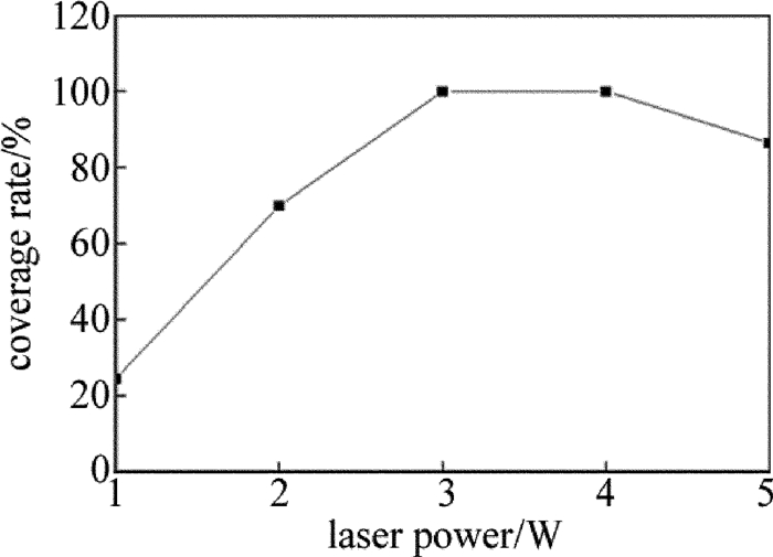
  • 取激光功率为1W~5W、光斑直径为2mm、扫描速率为5mm/s对基体进行扫描,激光功率对镀层覆盖率的影响如图 1所示。从图中可以看出,当激光功率为3W~4W时,镀层覆盖率为100%;激光功率小于3W时,镀层覆盖率随激光功率的增加而增大,这是由于激光功率逐渐升高使激光能量逐渐达到活化层中所有H2PO2-还原Ni2+所需的活化能,从而使镀层覆盖率逐渐增加;激光功率大于4W时,镀层覆盖率开始下降,这是由于激光功率的增加使光斑能量过大,瞬间高温会对陶瓷基体表面造成破坏,并使活性Ni微粒氧化而失去活性,从而使覆盖率下降。因此,为了节约能源,激光功率取为3W。

    Figure 1.  Relationship between laser power and coverage

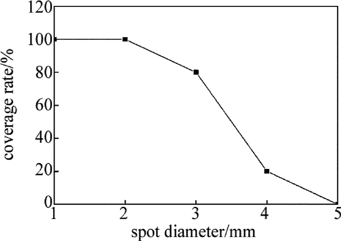
  • 取激光功率为3W、光斑直径为1mm~5mm、扫描速率为5mm/s对基体进行扫描,光斑直径对镀层覆盖率的影响如图 2所示。从图中可以看出,当光斑直径大于2mm时,镀层覆盖率开始下降,这是由于激光能量小于活化层中所有H2PO2-还原Ni2+所需的活化能,只有部分Ni2+被还原。因此,激光光斑直径取为2mm。

    Figure 2.  Relationship between spot diameter and coverage

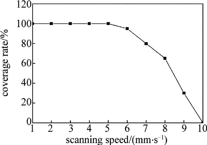
  • 取激光功率为3W、光斑直径为2mm、扫描速率为1mm/s ~10mm/s,扫描速率对覆盖率的影响如图 3所示。从图中可以看出,当扫描速率为1mm/s ~5mm/s时,镀层覆盖率为100%;扫描速率大于5mm/s时,镀层覆盖率开始下降,这是由于扫描速率越大,光斑在局部区域停留的时间越短,难以为活化层提供充足的反应能量,从而使覆盖率降低。因此,扫描速率取为5mm/s。

    Figure 3.  Relationship between scanning rate and coverage

  • 图 4为基体粗化后表面微观形貌。图中平均直径为10μm的孔为基体结构,其周围所分布的微孔为基体粗化所致。基体粗化后,亲水性明显提高,同时为活化液中活性离子的吸附提供了有利条件。

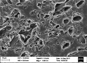
    Figure 4.  Surface morphology after matrix roughening

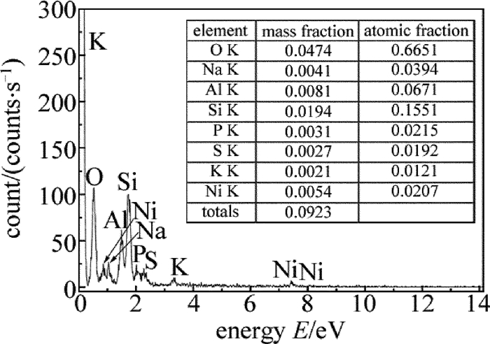
    图 5为基体活化后表面微观形貌。从图中可以看出,基体表面附着大量微粒状结构,平均直径为0.1μm。图 6基体表面活化能谱图。从图中可以看出,除基体所含有的元素外,还出现了Ni峰和P峰,质量分数分别为0.0054和0.0031,说明活化层中发生了无催化剂的化学镀镍反应,生成的活性Ni微粒附着在基体表面,使基体活化。

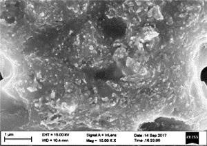
    Figure 5.  Surface morphology after matrix activation

    Figure 6.  Surface energy spectrum after matrix activation

    图 7为镀层表面微观形貌。从图中可以看出,镀层表面平滑,晶胞直径均在10μm以上,组织致密,结构紧凑。

    Figure 7.  Surface morphology of coating

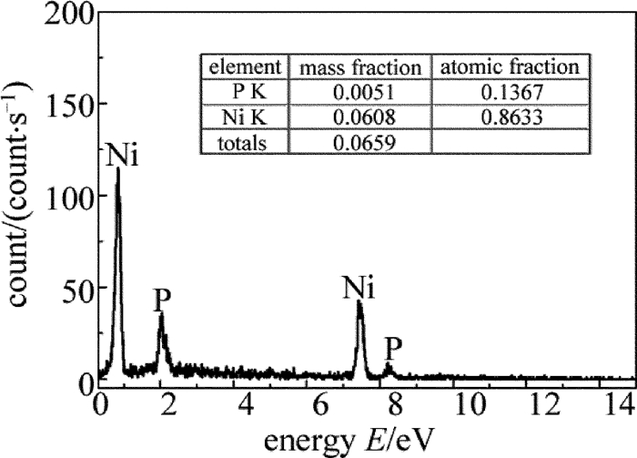
    图 8为镀层表面能谱图。图中只有Ni峰和P峰,说明基体被完全覆盖。Ni和P的原子数分数分别为0.8633和0.1367,计算得出镀层中P的质量分数为0.0771,为中磷化学镀层。

    Figure 8.  Surface energy spectrum of coating

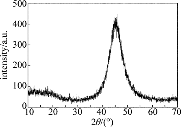
    图 9为镀层X衍射图谱。图中衍射峰均呈弥散状态,表明镀层结构为非晶态,具有良好的耐磨性和耐腐蚀性能[19-20]

    Figure 9.  X diffraction pattern of coating

  • 图 10为热震试验后样品实物图。将在最优工艺下施镀后的陶瓷基体放入200℃电烘箱中加热30min,然后迅速取出放入冷水中,重复实验3~4次,检测后样品表面光滑,无开裂、起包现象,说明镀层与基体表面结合力良好。

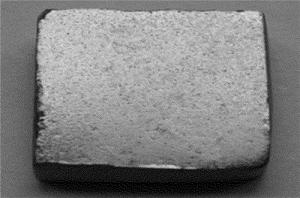
    Figure 10.  Sample physical map after binding test

  • 利用万用表测得试样电阻为0.3Ω,用晶相显微镜测得试样厚度为9.47μm。根据(1)式计算得到镀层电阻率ρ=7.67×10⁻⁵Ω·cm,导电性良好。

  • 图 11为常规可焊性检测前后对比图。以浸锡法对镀层进行点焊测试,观察锡焊点与镀层的润湿性均表现为良好且无明显差异;进行焊点拉脱强度测试,以强力拉拔使焊点脱落观察脱落点情况,焊点与基材分离,表明焊接强度良好。

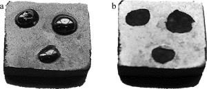
    Figure 11.  Contrast diagram of conventional weldability before and after testing

3.   结论
  • (1) 将10g/L NiSO4·6H2O和40g/L NaH2PO2混合溶液涂覆于基体表面,常温干燥8min ~10min,利用激光对基体进行均匀扫描。在激光热效应作用下,Ni2+被H2PO2-还原为平均直径为0.1μm的Ni微粒,使基体得到活化。

    (2) 激光最优参量如下:激光功率为3W,光斑直径为2mm,扫描速率为5mm/s。以最优参量对基体进行扫描,镀层覆盖率为100%。

    (3) 镀层中P的质量分数为0.0771,为中磷镀层,晶体结构为非晶态,具有良好的耐磨性和耐腐蚀性能。通过对镀层结合性、导电性以及可焊性的检测表明,镀层具有较好的综合性能。

    (4) 该工艺成本低、活化时间短、可操作性强,通过对扫描路径的控制能够实现基体的局部活化,同时能在基体表面成型各种精细图形,具有一定的使用价值。

Reference (20)

Catalog

    /

    DownLoad:  Full-Size Img  PowerPoint
    Return
    Return