Advanced Search

ISSN1001-3806 CN51-1125/TN Map

Volume 42 Issue 4
May  2018
Article Contents
Turn off MathJax

Citation:

Simulation of micronano fiber couplers based on fused drawing

  • Corresponding author: ZHU Yiqing, gyp@mail.ioa.ac.cn
  • Received Date: 2017-07-27
    Accepted Date: 2017-11-01
  • In order to study micronano fiber couplers, numerical simulation of the melting and drawing process of micronano fiber couplers was carried out by using beam propagation method. The curves of output light power with the change of tensile length and the distribution diagram of light field were obtained. The change of mode field and the characteristics of light field of three phases of the coupler were analyzed through software simulation. The results show that output light power of two fibers tends to be equal and no longer varies with the change of tensile length when a micronano fiber coupler is in the phase of losing the effective coupling. The characteristics of light field distribution of the fused taper coupler at various stages are different. The loss of effective coupling of taper-type micronano fiber coupler is directly related to fiber diameter of the melting zone. And the fiber diameter is related to the input light wavelength. The smaller the wavelength is, the smaller the fiber diameter that should be reached by the melt zone is. It is helpful for the study of the conditions for the loss of effective coupling of micronano fiber coupler.
  • 加载中
  • [1]

    TONG L, SUMETSKY M. Subwavelength and nanometer diameter optical fibers[M].Berlin, Germany:Springer, 2010:21-34.
    [2]

    ZHANG B, HOU J, JIANG Z F. Tellurite glass microstructured fibers for mid-IR supercontinuum generation[J]. Infrared and Laser Engineering, 2011, 40(2):328-331(in Chinese).
    [3]

    ZHANG L, ZENG Y, CHEN G Q, et al. Energy distribution of wedge-shaped micro/nanofiber[J]. Laser Technology, 2015, 39(5):689-693(in Chinese).
    [4]

    DING M, WANG P, BRAMBILLA G. A microfiber coupler tip ther-mometer.[J]. Optics Express, 2012, 20(5):5402-5410. doi: 10.1364/OE.20.005402
    [5]

    BO L, WANG P, SEMENOVA Y, et al. High sensitivity fiber refractometer based on an optical microfiber coupler[J]. IEEE Photonics Technology Letters, 2013, 25(3):228-230. doi: 10.1109/LPT.2012.2234449
    [6]

    YING Y H. Design of new kind of tunable micro ring resonator[J]. Infrared and Laser Engineering, 2016, 45(6):221-226.
    [7]

    YAN Sh B, ZHAO Y, YANG D Ch, et al. Optical tweezers based on near-field optical theory[J]. Infrared and Laser Engineering, 2015, 44(3):1034-1041(in Chinese).
    [8]

    CHEN G Y, ZHANG X L, BRAMBILLA G, et al. Enhanced responsivity of a flexural disc acceleration sensor based on optical microfiber[J]. Optics Communications, 2012, 285(23):4709-4714. doi: 10.1016/j.optcom.2012.02.099
    [9]

    DU Y, CHEN Zh, YU J H, et al. All micro-fiber polarization filter based on evanescent field coupling[J]. Chinese Journal of Lasers, 2012, 39(6):0610002(in Chinese). doi: 10.3788/CJL
    [10]

    BRAMBILLA G. Optical fibre nanowires and microwires:a review[J]. Journal of Optics, 2010, 12(4):043001. doi: 10.1088/2040-8978/12/4/043001
    [11]

    HONG Z, LI X, ZHOU L, et al. Highly-efficient optical power combiners based on evanescently-coupled micro/nano optical fibers[J]. Optics Communications, 2012, 285(17):3592-3596. doi: 10.1016/j.optcom.2012.04.024
    [12]

    WU F, WU B K, YU W Zh, et al. Design of fiber acoustic sensors based on 3×3 coupler phase demodulation[J]. Laser Technology, 2016, 40(1):64-67(in Chinese).
    [13]

    ZENG Y, ZHANG L, ZHOU A, et al. Investigation of coupling characteristics among three parallel micro/nano optical fibers[J]. Chinese Journal of Lasers, 2014, 41(9):0905003(in Chinese). doi: 10.3788/CJL
    [14]

    HONG Z, LI X, ZHOU L, et al. Coupling characteristics between two conical micro/nano fibers:simulation and experiment[J]. Optics Express, 2011, 19(5):3854-3861. doi: 10.1364/OE.19.003854
    [15]

    YU Y, ZHANG X L, XIE J H, et al. Investigation on fabrication and characteristics of four ports optical microfiber[J]. Chinese Journal of Lasers, 2015, 42(1):0105002(in Chinese). doi: 10.3788/CJL
    [16]

    BRAMBILLA G, XU F, FENG X. Fabrication of optical fibre nanowires and their optical and mechanical characterization[J]. Electronics Letter, 2006, 42(9):517-519. doi: 10.1049/el:20060611
    [17]

    JUNG Y, BRAMBILLA G, RICHARDSON D J. Optical microfiber coupler for broadband single-mode operation[J]. Optics Express, 2009, 17(7):5273-5278. doi: 10.1364/OE.17.005273
    [18]

    YU Y, ZHANG X L, SONG Zh Q, et al. Investigation on fabrication and vibration sensing properties of optical microfiber coupler[J]. Chinese Journal of Lasers, 2014, 41(11):1105002(in Chinese). doi: 10.3788/CJL
    [19]

    EISENMANN M, WEIDEL E. Single-mode fused biconical couplers for wavelength division multiplexing with channel spacing between 100 and 300nm[J]. Journal of Lightwave Technology, 1988, 6(1):113-119. doi: 10.1109/50.3975
    [20]

    REN J G, HU Y M, ZHANG X L, et al. A united model of fused single-mode fiber coupler[J]. Semiconductor Optoelectronics, 2011, 32(1):18-23(in Chinese).
    [21]

    LIN B, LIAN H, JIN M B. Optical waveguide calculation and discussion with finite-difference beam propagation method[J]. Chinese Journal Lasers, 2004, 31(s1):503-506(in Chinese).
  • 加载中
通讯作者: 陈斌, bchen63@163.com
  • 1. 

    沈阳化工大学材料科学与工程学院 沈阳 110142

  1. 本站搜索
  2. 百度学术搜索
  3. 万方数据库搜索
  4. CNKI搜索

Figures(6)

Article views(6488) PDF downloads(129) Cited by()

Proportional views

Simulation of micronano fiber couplers based on fused drawing

    Corresponding author: ZHU Yiqing, gyp@mail.ioa.ac.cn
  • 1. School of Science, Jiangnan University, Wuxi 214122, China
  • 2. School of Precision Instrument and Opto-electronics Engineering, Tianjin University, Tianjin 300129, China
  • 3. Suzhou Optoring Co. Ltd., Suzhou 215123, China

Abstract: In order to study micronano fiber couplers, numerical simulation of the melting and drawing process of micronano fiber couplers was carried out by using beam propagation method. The curves of output light power with the change of tensile length and the distribution diagram of light field were obtained. The change of mode field and the characteristics of light field of three phases of the coupler were analyzed through software simulation. The results show that output light power of two fibers tends to be equal and no longer varies with the change of tensile length when a micronano fiber coupler is in the phase of losing the effective coupling. The characteristics of light field distribution of the fused taper coupler at various stages are different. The loss of effective coupling of taper-type micronano fiber coupler is directly related to fiber diameter of the melting zone. And the fiber diameter is related to the input light wavelength. The smaller the wavelength is, the smaller the fiber diameter that should be reached by the melt zone is. It is helpful for the study of the conditions for the loss of effective coupling of micronano fiber coupler.

引言
  • 微纳光纤[1-3]通常是指直径在几微米及以下的光学波导, 具有强消逝场、强光约束、低损耗、尺寸小等特点[4-5],因而成为研究热点[6-7]。基于其独特的波导特性,微纳光纤耦合器的制作方法、器件特性和应用等[8-11]与常规的光纤耦合器[12]有着诸多的不同,近年来人们对它开展了多方面的研究工作。微纳光纤耦合器制作方法主要有基于消逝场耦合的微纳光纤搭靠法和熔融拉伸法,对于搭靠法制作微光纤耦合器,研究人员已经进行了相关理论和实验研究[13-14],而采用改进型的熔融拉锥平台拉制微光纤耦合器的实验研究相对较多[15-16],但理论研究较少。

    作者根据熔锥型光纤耦合器的复合波导特点,并考虑到拉制过程中耦合器波导结构的变化规律,建立了拉制微纳光纤耦合器过程中波导结构的变化模型。利用光束传播法对微纳光纤耦合器在熔融拉伸过程进行仿真模拟,计算得到输出光功率随拉伸长度变化的关系曲线以及在拉制过程中任何状态下耦合器的光场分布。由此看到耦合器熔融拉制到一定程度时,微纳光纤耦合器失去有效耦合,两输出端口的光功率相等且基本保持不变,与参考文献[17]和参考文献[18]中的实验曲线一致。通过对不同熔融区长度和不同输入光波长情况下耦合器的拉制过程仿真计算的结果进行对比分析,对微纳光纤耦合器失去有效耦合的成立条件进行了研究。

1.   几何模型建立
  • 将两根相同的光纤除去涂覆层并紧靠在一起,用高温加热熔融并向两侧拉伸,可以制作熔锥型光纤耦合器。根据耦合器横截面尺寸的特点,可将进行熔融拉锥的光纤分为熔融区、锥形区和非耦合区部分,P0为输入光功率,P1为直通臂输出光功率,P2为耦合臂输出光功率, 如图 1所示。

    Figure 1.  Model of micronano fiber coupler

    根据拉伸过程中光纤体积守恒,得单根熔锥光纤的纤芯直径和包层直径变化,可表示为[19]:

    式中,r表示未拉伸时光纤的纤芯直径,R表示未拉伸时光纤的包层直径,L表示拉伸长度,w表示熔融区的长度, zz轴方向长度。

    耦合器在熔融区和锥形区,两光纤达到不同程度的融合,形成的复合波导由两光纤的相互交叠而成,其横截面图如图 2所示。

    两根光纤间的融合程度称为熔融度α[20],定义为:

    式中, R(z)为光纤的包层直径,d为两纤芯间距。由上式可见,α=0时,d=R(z),即两光纤相切,未熔合;α=1时,$d=\left(\sqrt{2}-1 \right)R(z)$,即两光纤为全熔合状态。加热温度越高,熔融时间越长,两根光纤的熔融度越大。光纤通过较长时间熔融拉锥,最终形成微纳光纤耦合器,两光纤的熔融区已经达到全熔合状态,熔融度为1。

2.   模拟分析
  • 利用光束传播法[21](beam propagation method, BPM)通过差分方程加边界条件计算波导间的场分布,该方法具有简单方便、计算速度快、准确率高等优点,是光波导数值分析的主要方法之一。利用基于光束传播法的optiBPM软件,建立从常规光纤熔融拉制成微纳光纤耦合器的过程中波导结构的变化模型,并根据(1)式~(3)式编写相应的程序,就可以对耦合器的整个拉制过程进行模拟仿真。

    以SMF28光纤为例,取纤芯直径r=8.3μm、折射率n1=1.452,包层直径R=125μm、折射率n2=1.447。设熔融区长度为10000μm,输入光波长为λ=1550nm。

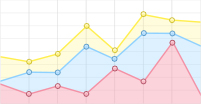
    图 3为耦合器两臂的归一化输出光功率随拉制长度L的变化曲线。其中port 1为直通臂归一化输出光功率P1/P0,port 2为耦合臂输出光功率P2/P0

    Figure 3.  The normalized output light power with the change of length L

    图 3可以看出,对于整个耦合器拉制过程,可以分为3个阶段,第一阶段,光在两光纤内随着拉制长度的增加呈周期性交替完全转移,且周期逐渐减小,常规光纤耦合器和波分复用器等光纤器件通常在这一阶段制作。第二阶段,两根光纤的输出光仍随拉伸长度呈交替增减,但交替周期更小、幅度出现波动,且光功率不再发生完全转移;当拉伸长度大约在60mm之后,由(1)式~(3)式可知,此时熔融区的光纤直径约小于4.5μm,两光纤的输出光功率接近相等,且基本稳定,不再随拉制长度的增加而发生交替变化,这一阶段的光纤耦合器为失去有效耦合的微纳光纤耦合器。此数值模拟结果与参考文献[17]和参考文献[18]中报道的通过实验得到的耦合器两光纤的输出光功率曲线图基本一致。

    用optiBPM软件模拟计算还可以得到耦合器在拉制过程中任何状态下的光场分布。

    图 4是不同拉伸阶段耦合器内的光场分布图。图 4a是第一阶段耦合器的光场分布,熔融区内的光场在两根光纤之间形成交替的100%完全转移;图 4b是第二阶段耦合器的光场分布,此时熔融区内的光场在两根光纤之间交替转移时,都会保留一些光场,出现不完全转移;图 4c为失去有效耦合的微纳光纤耦合器的光场分布,该阶段熔融区内的光场不再呈现出两根光纤内交替转移的特征,光可看成是在一根光纤内传输的。

    Figure 4.  Optical field distribution of coupler with different stretched stages

    另外从图 4还可以看出,拉伸长度比较小时, 光场分布在纤芯及其附近;但随着拉伸长度加大,光纤的锥形区和熔融区变的越细,原来在纤芯内传输的光场扩散到包层甚至空气中的也越多,引起附加损耗也就越大。因此,熔锥型微纳光纤耦合器的附加损耗相对比较大,这与图 3中得到的结果相一致。

3.   微光纤耦合器失去有效耦合的研究
  • 由上述论述可知,熔锥型光纤耦合器拉制时,如果熔融区拉的足够细,最终两输出臂的光功率会趋于相等并基本保持不变,此时微纳光纤耦合器失去有效耦合。以此为依据,研究失去有效耦合的微纳光纤耦合器的形成条件。

    设熔融区长度为15000μm,输入光波长为1550nm,进行数值模拟,得到两臂归一化输出光功率随拉制长度的变化曲线,如图 5所示。

    Figure 5.  The normalized output light power with the change of length L of the fused region

    图 5可知,拉伸长度大约为88mm,两臂输出光功率基本相等,此时微纳光纤耦合器失去有效耦合,根据(1)式~(3)式可以得出相应的光纤直径约为4.5μm。与上节模拟的熔融区长度为10000μm耦合器得到的结果相比较,在光波长相同的情况下,微纳光纤耦合器是否达到失去有效耦合的状态,取决于光纤直径大小,与熔融区长度和拉伸长度无关。

    设置输入光波长为900nm,熔融区长度为10000μm,进行数值模拟,得到两臂归一化输出光功率随拉制长度L的变化曲线,如图 6所示。

    Figure 6.  The normalized output light power with the change of input light wavelength

    图 6可见,输入光波长为900nm时,达到失去有效耦合的微纳光纤耦合器状态所需拉伸长度大约为70mm,根据(1)式~(3)式可以得出对应的光纤直径分别为2.7μm。与上节中的模拟结果比较,微纳光纤耦合器失去有效耦合与输入光波长有一定关系,输入光波长越小,熔融区的光纤直径越小。

4.   结论
  • 建立从常规光纤熔融拉制成微纳光纤耦合器的过程中波导结构的变化模型,利用光束传播法对耦合器整个拉制过程进行模拟仿真,得到输出光功率随拉伸长度变化的曲线图以及在拉制过程中任何状态下耦合器的光场分布。由此看出,光纤耦合器的拉制过程可以分成3个阶段:第一阶段,光在两光纤内随着拉制长度的增加呈周期性交替, 出现100%的转移,且周期逐渐减小;第二阶段,光在两根光纤内仍随拉伸长度呈交替增减,但交替周期更小、交替幅度出现波动,光功率出现不完全转移,且振荡周期越来越小;第三阶段为微纳光纤耦合器失去有效耦合阶段,两光纤的输出光功率接近相等且基本稳定,不再随拉制长度的变化而变化,此时光纤直径在微米数量级。通过对不同熔融区长度和不同波长输入光的情况下耦合器的拉制进行仿真模拟分析,对失去有效耦合的微纳光纤耦合器形成条件进行了研究分析。研究发现, 微纳光纤耦合器是否达到失去有效耦合的状态与熔融区的光纤直径直接关联的,与熔融区长度和拉伸长度没有本质关系;但此光纤直径与输入光的波长有关,波长越小,熔融区需经拉伸达到的光纤直径越小。

Reference (21)

Catalog

    /

    DownLoad:  Full-Size Img  PowerPoint
    Return
    Return