Advanced Search

ISSN1001-3806 CN51-1125/TN Map

Volume 41 Issue 4
May  2017
Article Contents
Turn off MathJax

Citation:

Optimal design of crosstalk in 4×10Gbit/s parallel optical modules

  • Corresponding author: ZHANG Keifei, zhangkefei67@163.com
  • Received Date: 2016-08-29
    Accepted Date: 2016-11-28
  • In order to realize crosstalk optimization of 4×10Gbit/s parallel optical modules, by using the ABCD transfer matrix method, combining with the optical fiber coupling constraint and the theory of collimating lens, focus lens and fiber end surface of the ball lens, two sets of optimization schemes were designed. Beam characteristics of vertical cavity surface emitting lasers (VCSEL) were studied, the relationship between the spot radius and divergence angle was simulated by using MATLAB, and crosstalk situation was analyzed. Optical modeling in ZEMAX non-sequential mode was founded, the parameters of lens structure and the design of fiber end face were optimized. After theoretical analysis and experimental verification, the optimized coupling beam radius and coupling efficiency were obtained. The results show that in indirect coupling optimization structure, light spot at the end of fiber is 53.72μm, coupling efficiency is up to 72.59%. In direct coupling optimization structure, light spot at the end of fiber is 3.695μm, and coupling efficiency is up to 76.11%. The design effectively solves the problem of optical crosstalk between parallel optical modules. The study is helpful for the optimization of transmission quality of optical network signal.
  • 加载中
  • [1]

    JIA J Ch, CHEN H D, PEI W H, et al. Vertical cavity surface emitting laser in very short distance (VSR) twenty anniversary of the establishment of the parallel application[C]// Optical Transmission System in China Optical Society of Photoelectric Technology Specialized Committee and the National Conference on Optoelectronic Technology and System. Beijing: China Optical Society, 2005: 17-33(in Chinese).
    [2]

    CHEN C T, HSIAO H L, CHANG C C, et al. 4 channels×10-Gbps optoelectronic transceiver based on silicon optical bench technology[J]. Proceedings of the SPIE, 2012, 8267: 82670D.
    [3]

    HU W, ZHOU B J, LI H Y, et al. Development of a 120Gbit/s very short distance parallel optical module[J]. Semiconductor Optoelectronics, 2015, 36(6): 964-967(in Chinese).
    [4]

    CHEN Y Q, WANG J H. Laser principle[M]. 2nd ed. Hangzhou: Zhejiang University Press, 2010: 101-107(in Chinese).
    [5]

    LI W Ch, GU J Q, WANG Y P. Study on measurement of laser beam and beam waist spot size[J]. Journal of Tianjin University (Science and Technology Edition), 2002, 23(3): 358-361(in Chinese).
    [6]

    CHEN H D. Very short distance optical transmission technology. Beijing: Science Press, 2005:87-90(in Chinese).
    [7]

    LI P. Research on micro lens optical fiber coupling technology of semiconductor laser[D]. Hangzhou: Zhejiang University, 2006: 78-119(in Chinese).
    [8]

    KATAOKA K. Estimation of coupling efficiency of optical fiber by far-field method[J]. Optical Review, 2010, 17(17):476-480.
    [9]

    DU Ch L, ZHOU Ch X. Design of beam collimation and focusing system for semiconductor laser array[J]. Optical Instrument, 2000, 22(6): 25-29(in Chinese).
    [10]

    YAN CH L, LU P, LIU D M, et al. Design and loss analysis of micro lens array coupled with optical fiber array[J]. Journal Optoelectronic Laser, 2006, 17(9): 1043-1047(in Chinese).
  • 加载中
通讯作者: 陈斌, bchen63@163.com
  • 1. 

    沈阳化工大学材料科学与工程学院 沈阳 110142

  1. 本站搜索
  2. 百度学术搜索
  3. 万方数据库搜索
  4. CNKI搜索

Figures(14)

Article views(3135) PDF downloads(299) Cited by()

Proportional views

Optimal design of crosstalk in 4×10Gbit/s parallel optical modules

    Corresponding author: ZHANG Keifei, zhangkefei67@163.com
  • 1. College of Science, Southwest University of Science and Technology, Mianyang 621010, China
  • 2. College of Science and Technology, Southwest University of Science and Technology, Mianyang 621010, China

Abstract: In order to realize crosstalk optimization of 4×10Gbit/s parallel optical modules, by using the ABCD transfer matrix method, combining with the optical fiber coupling constraint and the theory of collimating lens, focus lens and fiber end surface of the ball lens, two sets of optimization schemes were designed. Beam characteristics of vertical cavity surface emitting lasers (VCSEL) were studied, the relationship between the spot radius and divergence angle was simulated by using MATLAB, and crosstalk situation was analyzed. Optical modeling in ZEMAX non-sequential mode was founded, the parameters of lens structure and the design of fiber end face were optimized. After theoretical analysis and experimental verification, the optimized coupling beam radius and coupling efficiency were obtained. The results show that in indirect coupling optimization structure, light spot at the end of fiber is 53.72μm, coupling efficiency is up to 72.59%. In direct coupling optimization structure, light spot at the end of fiber is 3.695μm, and coupling efficiency is up to 76.11%. The design effectively solves the problem of optical crosstalk between parallel optical modules. The study is helpful for the optimization of transmission quality of optical network signal.

引言
  • 数字化进程的飞速发展对带宽提出更高需求,短距互联成为数字系统传输领域的关注热点。并行光互连利用并行光模块和带状光缆来实现。并行光输出模块是高速光互联传输领域中的关键器件之一,其耦合效率、光束串扰等因素直接影响光信号的传输质量和系统性能。

    2005年JIA等人在全国光电技术与系统学术会议[1]介绍了以垂直腔面发射激光器(vertical cavity surface emitting laser, VCSEL)为基础器件的高速大容量、高并行处理光收发模块系统,国外采用的两种光路结构,一种是激光器发出的光直接进入45°斜面光纤,一种是激光器发出的光,通过一个反射镜反射进入光纤,这两种方式也是目前商用模块中常用结构。但其都未考虑阵列光源相邻光束间的影响。2012年, CHEN等人设计了4个通道并行传输模块[2],采用柔性的印制电路板(printed carcuit board, PCB)让光源直接和光纤非常近的距离耦合,这样做不仅可以很明显地降低光串扰,而且耦合效率高、插入损耗低,但对在PCB板上进行电路布局增加了难度,而且制作柔性的PCB板成本非常高,工程上应用较困难。2015年, HU等人设计了12个通道,单通道10Gbit/s的120Gbit/s并行光传输模块[3],其光路部分采用45°棱镜进行光路传播方向改变,且在光进入棱镜和出射处集成了准直和聚焦透镜,这对工艺要求提高了更多,成本上也大大增加。

    作者针对4×10Gbit/s并行光模块常用的两种光耦和结构特点,结合实际生产需要设计了两种优化方案。运用光学元件,压缩并行光模块之间的光束,使之相互独立,有效解决光模块串扰问题。实现了并行光模块的低成本生产、高效率传输, 更适合市场需求。

1.   激光器特性分析
  • VCSEL激光光束服从高斯分布,沿z轴传播的光束近似看成沿z轴传播的基模高斯光束,基模高斯光束可表示为[4]

    式中,等号右边第1项为振幅因子,第2项为纵向相位,第3项为径向相位。k为波数,r为光束到光轴的距离。由该式可得出基模高斯光束的几个关键参量:

    式中, w(z)为光斑半径; w0为最小光斑尺寸,即束腰; R(z)为等相面的曲率半径; z0为高斯光束的共焦参量。

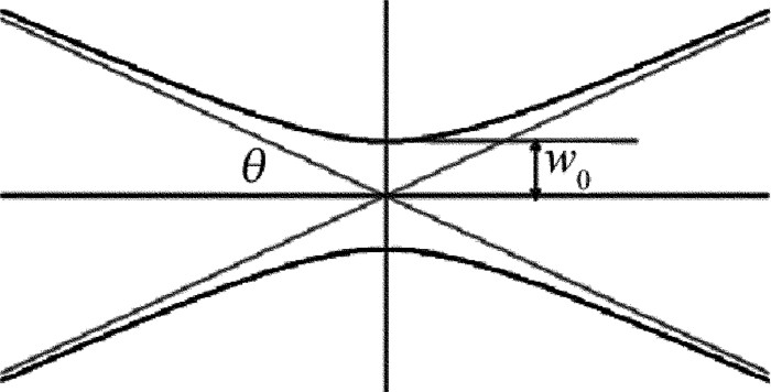
    定义光束发散角θ为在瑞利距离外,高斯光束振幅缩减为激光中心最大值1/e2处,远场处高斯光束与z轴夹角。定义基模高斯光束光斑半径w(z)振幅按高斯规律减小到中心值的1/e处的r值大小[5], 如图 1所示。

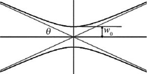
    Figure 1.  Propagation of Gaussian beam

    所以发散角与光斑半径为:

  • 通常在计算激光器的光强分布时,所用公式为:

    式中, αxαy是激光光束发散角,单位为°; θxθy为发散角变量,θx′, θy′为θx, θy的半峰全宽; GxGyxy方向的超高斯因子,GxGy要求必须大于0.01,如果GxGy等于1.0,则产生一个典型的高斯分布。

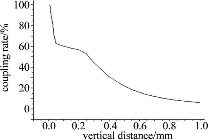
  • 在ZEMAX中通过改变激光器与光纤位置参量,进行光线追迹,查看探测器给出数据,得到随着激光器与光纤距离的增加,系统耦合效率将降低,具体耦合效率随距离的变化, 如图 2所示。

    Figure 2.  Relationship between coupling efficiency and axial distance

    可知当耦合距离达到1mm时,耦合效率低至6.09%,严重影响通信质量,器件几乎不能使用。所以,VCSEL激光器与光纤多使用间接耦合系统。
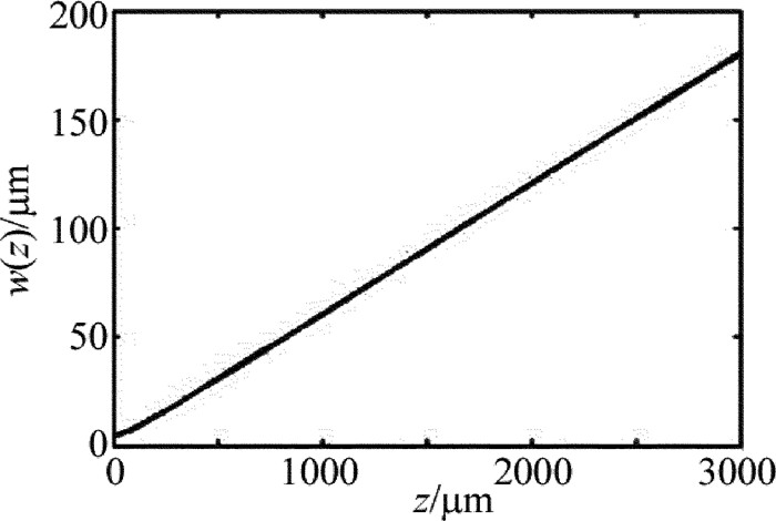
  • 图 3所示,根据高斯光束光斑半径w(z)随传播距离z的函数,并用MATLAB软件进行处理:

    Figure 3.  Relationship between spot radius w(z) and propagation distance z

    为了方便计算,λ取波段840nm~860nm的中值850nm。光束束腰w0取为4.5μm。

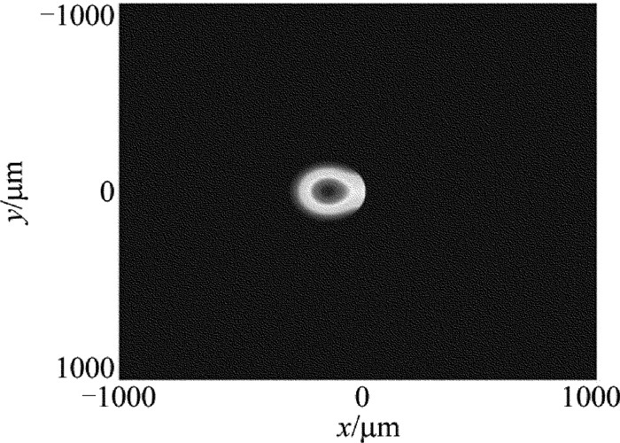
    根据实际激光器的相关参量,设定激光发散角为20°,光源到光纤端面距离为3mm,分析可得在并行光模块中光束传播到光纤端面时光斑大小为320.92μm。在MATLAB软件中建立两束光束,光束中心间距为250μm,得到两束光束传播到3mm处时的光斑图,如图 4所示。高斯光束光强有效值取为2mW/μm2,单光束对相邻光束的影响如图 5所示。经过计算得到, 来自相邻光束的光强为0.17mW/μm2

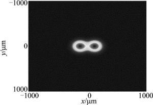
    Figure 4.  Speckle pattern when adjacent beam propagating 3mm

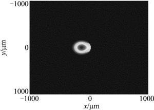
    Figure 5.  Effect of beam crosstalk

    在光接收机部分,光检测器检测到调制后的光信号,通过放大器进入解调器,解调器通过判决光检测器所产生的电信号幅值是比特1还是0,从而完成对光的解调[6]。光检测器检测到的功率大于理论值,探测器接收到的光子数目相比理论值要多,使得探测器产生比特1和0信号的时间相对理论值存在误差,那么解调器进行判决时相对理论值存在差错,最终将导致信号传输过程中产生噪声和误码现象。其次,光斑发散,会使部分能量在耦合时丢失,耦合效率降低。

2.   并行光模块耦合结构及优化
  • 由于VCSEL激光器出射光束垂直于安装的PCB板的表面,在工程应用中常有直接与间接耦合两种结构。

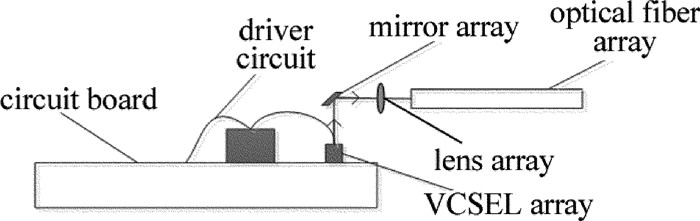
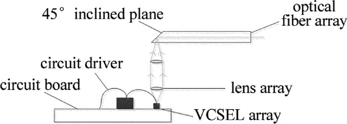
  • 为了使垂直出射的阵列光耦合进入平行的带状光纤, 将模块光接口的方向平行于电路板方向,通过使电信号或者光信号在传输的过程中进行一个90°的转变,从而实现耦合电弯折将VCSEL光源发出的光束照射到45°斜面光纤上,通过斜面反射进入光纤,实现光的90°偏转,如图 6所示。光弯折则是利用柔性电路板弯折90°,然后激光器发出的光直接射入光纤,从而实现光的90°偏转,如图 7所示。工程上多采用电弯折方式,主要原因一是在柔性电路板上进行电路布局是非常复杂的,而且在电路上容易产生电路串扰,二是柔性电路板采用材料在成本上比普通电路板更高。

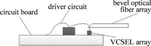
    Figure 6.  Schematic diagram of electric bending and coupling

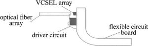
    Figure 7.  Schematic diagram of optical bending and coupling
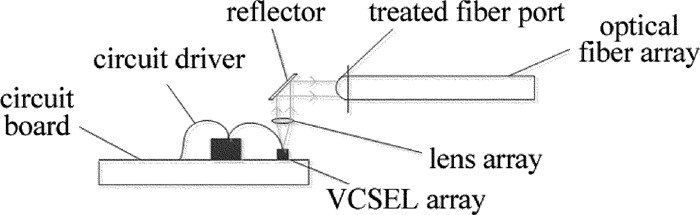
  • 间接耦合光路原理[6]图 8所示。激光器阵列发出的光通过一个45°反射镜或者棱镜实现光路90°偏转。此方式延长了耦合距离,加上激光光束发散程度随着传播距离的增加成线性增长,使得在耦合时很大一部分光能量丢失,而且相邻光束间的串扰对系统的影响更加明显。

    Figure 8.  Schematic diagram of indirect coupling

  • 优化设计是为了光束在传播的过程中彼此独立不干扰,即是相邻光束光斑在传播过程中满足串扰约束条件,就可以避免光束串扰对系统造成影响。设计目的为优化激光器阵列和光纤阵列的光路结构,从而降低光速串扰对系统的影响,为降低计算复杂度和设计工作量,研究通过从分析单管系统扩展到阵列系统。

  • 对于直接耦合光路结构中的串扰,通过设计准直透镜和聚焦透镜对光束聚焦[7-8],在光束传播的过程中降低光束的发散程度,使相邻光束都只是在自己独立的通道上传输,从而减小相邻光束的串扰,如图 9所示。

    Figure 9.  Schematic diagram of direct coupling junction

  • 间接耦合系统通过反射镜的方式延长了光传播距离,根据第2.2节中的分析,光束传播距离越长,光束串扰越严重,考虑到间接耦合的结构要求,本文中设计3个系统改善其串扰的影响。第1个系统为光源的准直系统[9],考虑到激光光束的发散角很大,避免光束串扰的影响,所以设计准直系统压缩光束发散角。第2个系统为光束传播方向偏转系统,使光束传播方向实现90°偏转。第3个系统为光纤端面设计系统,是光束易于和光纤耦合,保证耦合效率并降低相邻光束间的串扰,如图 10所示。

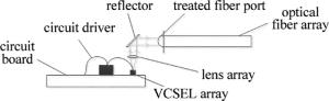
    Figure 10.  Schematic diagram of indirect coupling structure

3.   光路建模
  • 直接耦合优化设计中,添加聚焦透镜对光束进行聚焦,通过ZEMAX进行阵列建模,建立的模型如图 11所示。

    Figure 11.  Optical path structure of direct coupled array

  • 间接耦合结构中光路串扰优化建模与直接耦合结构光路串扰优化建模同理。其改变光束传播方向的是反射镜,在并行光模块中为了工艺加工方便,针对整列光束的反射系统,不是由多个反射镜并行构成阵列形成反射镜,一般由一块大的反射镜直接构成。

    通过ZEMAX进行间接耦合阵列光路建模,建立的模型如图 12所示。

    Figure 12.  Optical path structure of indirect coupling array

4.   优化结果分析
  • 在纯非序列系统中,利用探测器进行光线追迹,可以在探测器查看器中查看各个光束的辐射强度情况和辐射面积。探测前首先清除探测器探测杂散光等,然后进行光线追迹。下面将分别利用探测器探测直接耦合光路和间接耦合光优化后的阵列光束光强辐射情况。

    图 13图 14分别为直接耦合光路与间接接耦合光路优化后光纤端面光辐射图。两组图中右图中横坐标为线整列光斑的相对位置,单位为mm;纵坐标为辐射功率密度,单位为W·cm-2,两组图的总光功率都为3.9959W。其中耦合光路中,探测器探测到尖端平均光功率分别为9.2509×10⁴W/cm2和1.7549×104W/cm2

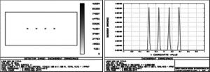
    Figure 13.  Optical radiation patterns of the optimized direct coupling optical fiber end face

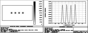
    Figure 14.  Optical radiation patterns of the optimized indirect coupling optical fiber end face

    可以看出,直接耦合结构与间接耦合结构优化后的光束在光纤端面形成的光斑都是彼此独立的,且非常均匀,利用探测器探测并计算得到各个光束中心光斑大小和耦合效率。其中直接耦合结构的光斑半径为3.695μm,耦合效率为76.11%;间接耦合结构的光斑半径为53.72μm,耦合效率为72.59%。

5.   结论
  • 在非序列模式下得到的数据与理论计算得出的数据和ZEMAX在序列模式下得到的数据具有较大出入,主要原因为非序列模式下没有优化各器件的位置距离等导致。但从图中仍可以看出,通过优化后,并行光模块中阵列光束在光纤端面的光斑大小不仅小于相邻光源的中心间距,也小于光纤的纤芯直径,满足耦合条件,且优化后的光路提高了光束与光纤的耦合效率。

    以上设计和实验都是基于理想情况,没有考虑光源与光纤的耦合损耗等情况,根据已有研究成果可知,在进行微透镜阵列和光纤阵列耦合时,一定要减小角度偏斜以减少角度偏斜误差,并且保证光源与光纤的横向、纵向偏移非常小,才能获得高的耦合效率[10]

Reference (10)

Catalog

    /

    DownLoad:  Full-Size Img  PowerPoint
    Return
    Return