Advanced Search

ISSN1001-3806 CN51-1125/TN Map

Volume 41 Issue 3
Mar.  2017
Article Contents
Turn off MathJax

Citation:

Research of temperature field and thermal stress field of CCD under laser irradiation

  • Corresponding author: NIU Yanxiong, niuyx@buaa.edu.cn
  • Received Date: 2016-06-03
    Accepted Date: 2016-07-29
  • In order to study interaction process and damage mechanism between laser and CCD sensors, an interline transfer surface array CCD irradiated by 1.06μm CW laser was analyzed and simulated by means of finite element analysis. Thermal coupling model was established by using laser irradiation area of substrate Si surface as heat source. The temperature distribution and thermal stress distribution of CCD were simulated. By comparing and analyzing temperature damage and stress damage of the components, it was found that stress damage was prior to temperature damage. The results show that as the convergence of the fixed boundary and the free boundary, the thermal stress at the edge of the lower surface of the base Si is the first to exceed the damage threshold of 120MPa at the time of laser action of 0.1s, and stress failure occurs. Si material slips from the lower surface edge to the center, and the substrate is gradually out of fix. At the time of laser action of 0.3s, stress failure occurs to Al film and SiO2 film and Al film strips radically from the inside to the outside due to thermal stress over the adhesion strength of 100MPa, finally the CCD is out of work position and fails. The research achievements provide theoretical basis for laser damage and protection of CCD sensors.
  • 加载中
  • [1]

    LIU G H. Research on the TV tracking system technology[D]. Nanjing: Nanjing University of Science and Technology, 2013: 1-2(in Chinese).
    [2]

    ZHANG L P. The hardware design and realization of TV tracking[D]. Wuhan: Wuhan University of Science and Technology, 2008: 1-2(in Chinese).
    [3]

    BI J, ZHANG X H, NI X W. Mechanism for long pulse laser-induced hard damage to the MOS pixel of CCD image sensor[J]. Acta Physica Sinica, 2011, 60(11):114210(in Chinese).
    [4]

    ZHANG D Y, ZHAO J H, WANG W P, et al. Study of disturance to visible-light array CCD detectors irradiated by 1.319μm CW YAG laser[J].High Power Laser and Particle Beams, 2003, 15(11):1050-1052(in Chinese).
    [5]

    GUO Sh F, CHENG X A, FU X Q, et al.Failure of array CCD irradiated by high-repetitive femto-second laser[J]. High Power Laser and Particle Beams, 2007, 19(11):1783-1786(in Chinese).
    [6]

    CHENG X A, LU Q Sh, MA L Q, et al. Experimental study of HgCdTe(PV) detector irradiated by CW 1.319μm laser[J]. Acta Optica Sinica, 2003, 23(5):622-626(in Chinese).
    [7]

    ZHANG Ch, WANG B, LIAO Zh Y, et al.Experimental study on disturbing effect of pulsedlaser against array CCD imaging systems[J].Laser Technology, 2014, 38(5):619-622(in Chinese).
    [8]

    NI X W, LU J, HE A Zh. Study of hard-destructive mechanism of the charge-coupled devices by a laser[J].Acta Physica Sinica, 1994, 43(11):1795-1802(in Chinese).
    [9]

    QIU D D, ZHANG Zh, WANG R, et al. Mechanism research of pulsed-laser induced damage to CCD imaging devices[J].Acta Optica Sinica, 2011, 31(2):0214006(in Chinese). doi: 10.3788/AOS
    [10]

    SINGH A P, KAPOOR A, TRIPATHI K N, et al. Laser damage studies of silicon surfaces using ultra-short laser pulses[J]. Optics & Laser Technology, 2002, 34(1):37-43.
    [11]

    LIU X, DU D, MOUROU G. Laser ablation and micromachining with ultrashort laser pulses[J]. IEEE Journal of Quantum Electronics, 1997, 33(10):1706-1716. doi: 10.1109/3.631270
    [12]

    NIE J S, WANG X, LI H, et al. Thermal and mechanical damage in CCD detector induced by 1.06μm laser[J].Infrared and Laser Engineering, 2013, 42(s2):380-386(in Chinese).
    [13]

    YONEMOTO K. CCD/CMOS image sensor no Kiso to Ouyou[M].Beijing:Science Press, 2006:65-76(in Chinese).
    [14]

    LU J, NI X W, HE A Zh.Physics of interaction between laser and materials[M]. Beijing:Machinery Industry Press, 1996: 32-34(in Chinese).
    [15]

    SUN Ch W. Laser irradiation effect[M].Beijing:National Defend Industry Press, 2002:28-32(in Chinese).
    [16]

    LIN B P, TANG J N, LIU H J, et al.Structure and infrared emissivity of polyimide/mesoporoussilica composite films[J].Journal of Solid State Chemistry, 2005, 178(3):650-654. doi: 10.1016/j.jssc.2004.12.010
    [17]

    SHAO C M, LUO Y, XU G Y, et al.Preparation and infrared emissivity properties of core-shell structured SiO2@ Bi2O3 spheres[J].Materials Science & Technology, 2010, 18(1): 43-45(in Chinese).
    [18]

    WANG X L.Preparation and properties of PI/SiO2-Al2O3 nanocomposite films[D].Harbin: Harbin University of Science and Technology, 2009: 4-5(in Chinese).
  • 加载中
通讯作者: 陈斌, bchen63@163.com
  • 1. 

    沈阳化工大学材料科学与工程学院 沈阳 110142

  1. 本站搜索
  2. 百度学术搜索
  3. 万方数据库搜索
  4. CNKI搜索

Figures(6) / Tables(1)

Article views(7182) PDF downloads(18) Cited by()

Proportional views

Research of temperature field and thermal stress field of CCD under laser irradiation

    Corresponding author: NIU Yanxiong, niuyx@buaa.edu.cn
  • School of Instrument Science and Opto-electronics Engineering, Beihang University, Beijing 100191, China

Abstract: In order to study interaction process and damage mechanism between laser and CCD sensors, an interline transfer surface array CCD irradiated by 1.06μm CW laser was analyzed and simulated by means of finite element analysis. Thermal coupling model was established by using laser irradiation area of substrate Si surface as heat source. The temperature distribution and thermal stress distribution of CCD were simulated. By comparing and analyzing temperature damage and stress damage of the components, it was found that stress damage was prior to temperature damage. The results show that as the convergence of the fixed boundary and the free boundary, the thermal stress at the edge of the lower surface of the base Si is the first to exceed the damage threshold of 120MPa at the time of laser action of 0.1s, and stress failure occurs. Si material slips from the lower surface edge to the center, and the substrate is gradually out of fix. At the time of laser action of 0.3s, stress failure occurs to Al film and SiO2 film and Al film strips radically from the inside to the outside due to thermal stress over the adhesion strength of 100MPa, finally the CCD is out of work position and fails. The research achievements provide theoretical basis for laser damage and protection of CCD sensors.

引言
  • 随着光电技术的发展,CCD作为一种图像传感器,以其体积小、数字化、速度快、寿命长等优点[1],已成为电视跟踪、光电成像、光电观瞄等系统的重要组成部分。由于CCD是一种弱光成像器件,在受到激光光源辐照时,一方面激光使CCD光敏单元的光电转换达到饱和,使成像受到干扰;另一方面激光在与组成CCD材料的作用过程中,会造成不可逆的损伤破坏[2]。因此,研究激光辐照CCD的温度分布与应力分布对丰富激光损伤机理数据库以及改善CCD抗激光加固措施[3],从而制造成相应的激光压制武器及激光防护装置有着重要意义。

    激光辐照会造成CCD光饱和、灵敏度退化、伏安特性曲线变直及暗电流产生等光学、电学性能下降的软破坏[4-7]。而更严重的是,激光辐照产生的热学效应及力学效应会使CCD的组成材料及结构发生不可逆的硬破坏[8-11],致使CCD永久失效。针对这方面的研究,国内外已有很多报道,主要方法分为实验研究和仿真研究两种。在仿真研究中,大多数学者认为CCD受激光辐照时,金属遮光层和感光层均与激光发生作用[3, 12],忽略了微透镜对激光辐照位置的影响;并且,在仿真中将CCD的各面作为自由边界处理,忽略了真实环境中基底要固定的实际情况;计算过程中,忽略了热传导及热辐射,热辐射是关于靶材温度4次方的函数,在靶材温度逐渐升高的过程中,热辐射对靶材温度的影响会越来越大。

    本文中由激光辐照的实际位置出发,建立了热力耦合模型。以波长为1.06μm、功率0.5W的连续激光辐照CCD进行仿真研究,首次将热辐射、热对流及固定约束等实际条件纳入到激光对CCD辐照的仿真中,依据仿真结果,讨论了CCD的硬破坏机理。

1.   理论模型
  • CCD按入射光线方向组成材料依次为微透镜、SiO2增厚层、金属遮光Al膜层、SiO2绝缘层、基底Si[13]。构成微透镜的主要材料为聚酰亚胺(polyimide,PI),材料PI及SiO2对1.06μm的激光吸收率几乎为0,全部光能被微透镜通过金属层开口聚焦到基底Si表面,金属层不受激光辐照。基底Si对1.06μm的激光有较强的吸收率η=67%,因此可以将激光辐照CCD看成是CCD基底Si上加了一个热源。基于这种思想,对CCD进行简化,并进行理论分析与仿真。将CCD简化为圆形结构靶材,如图 1所示。

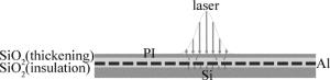
    Figure 1.  The simplified model of CCD

  • 假设各层材料均为各向同性均匀,热传导和热弹性耦合的基本方程组可描述为[3]

    式中, Tj为第j层材料在t时刻的温度分布;ρjcjκjDj分别表示材料的密度、比热容、导热系数和热扩散率;Qj是体热源,表示激光作用下材料所吸收的激光能量;urjuzj分别表示位移在径向和轴向上的分量;εj, μj, βj分别表示体应变、泊松比和材料的热膨胀系数;j=PI,Ot,M,Oi,Si, 分别表示微透镜、SiO2增厚层、金属遮光层、SiO2绝缘膜层、基底Si。其中Qj可以表示成以下形式[14]

    (1) 当为基底Si层时,激光能量在Si表面被吸收,可简化看成基底Si层上表面有一热源,这样QSi就可改为边界条件中面热源来表示:

    式中, ηSi表示基底Si对激光的吸收率,I0表示激光光斑中心的功率密度,w表示高斯光斑的束腰半径,r表示考察点到光斑中心的径向距离。

    (2) 当为其它层时,热量是从基底Si层上表面热传导来的,因此对应的边界条件为:

    式中, hj(j=Si, Oi, M, Ot, PI)表示各层材料的厚度,K表示外表面和空气的对流传热系数,αPI为微透镜的发射率,σ为黑体辐射常数,Tair为环境温度。为了得到激光辐照CCD的温度场及应力场,采用有限元法能有效地处理各种复杂边界条件。

2.   仿真分析
  • 根据上述理论模型,使用波长为1.06μm、功率0.5W的连续激光对CCD进行照射,光斑半径a=1mm,光斑的功率密度分布如图 2所示。初始环境温度Tair=300K,CCD底部为固定约束,并假设底部绝热,四周与空气形成对流,对流传热系数K=5W/(m2·K)。激光辐照下,把CCD内各材料间的辐射换热看成是热传导的一部分,而设CCD向外界辐射换热主要由最上层上表面进行,且辐射能量主要集中在红外波段,忽略其它波段的辐射能量损失。当激光辐照开始时,主要由微透镜上表面进行辐射换热,当微透镜层达到一定温度发生热分解后,辐射换热由SiO2增厚层上表面与环境进行。组成CCD的各种材料参量见表 1

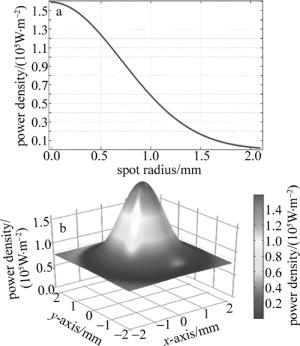
    Figure 2.  Power density distribution of the spot

    parameter PI Al SiO2 Si
    density ρj/ (kg·m-3) 1.53×10³ 2.7×10³ 2.64×10³ 2.52×10³
    thermal conductivity κj/(W·m-1·K-1) 0.12 238 1.3 156
    melting point Tm, j/℃ 500(pyrolysis) 660 1700 1412
    specific heat capacity cj/(J·kg-1·K-1) 1.09×10³ 1.05×10³ 841 1009
    thermal expansion coefficient βj/K-1 2×10⁻⁵ 2.29×10⁻⁵ 5×10⁻⁷ 2×10⁻⁵
    Young’s modulus Ej/Pa 4×10⁹ 1.38×10¹¹ 8.7×10¹⁰ 1.07×10¹¹
    Poisson’s ratio μj 0.3 0.33 0.16 0.28
    thickness hj/μm 2 1 thickening 3.2 insulation 0.2 30
    radius rj/mm 2.4 2.4 2.4 2.4
    emissivity αj 0.521 0.985
    absorption rate of 1.06μm laser ηj 0.06 0.67

    Table 1.  CCD components[3, 15-18]

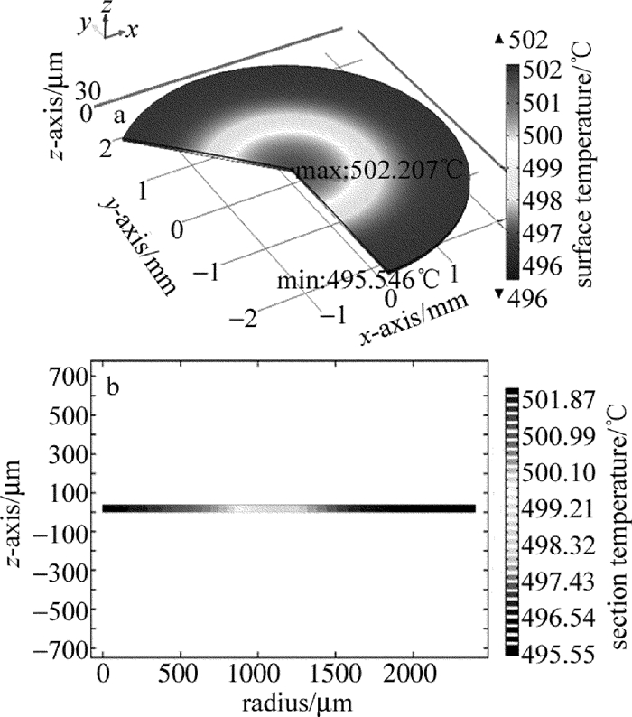
  • 图 3为CCD在激光辐照时刻t=3.4s时的温度分布图。由图可知,温升从激光光斑中心向靶材边缘递减,而沿轴向变化不大,沿径向有大约6℃的温差。因此,研究CCD的热损伤时可以计算CCD的平均温度。

    Figure 3.  Material temperature distribution at t=3.4s

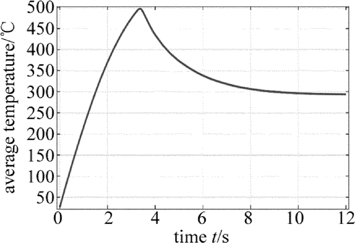
    图 4为CCD的平均温度与辐照时间的关系。由图可知,随着辐照时间的增加,温升逐渐增加,但是增速逐渐趋缓。这是因为随着CCD整体的温度升高,辐射换热量也逐渐增大,能量损耗的加大使温度曲线呈现为“上凸”式上升,当t=3.4s,CCD温度达到500℃,微透镜热分解,假设PI全部分解,忽略其分解作用时间。微透镜分解后聚光效应消失,激光透过SiO2增厚层照射到遮光Al膜上,一般Al膜开口率30%,也就是说激光能量的70%作用在Al膜上,其余30%继续作用在基底Si上。由于Al膜对该波段激光吸收率仅6%,激光的大部分能量被反射,CCD中整体的输入热源大幅降低,再加上SiO2增厚层的热辐射系数比PI高很多,所以温度曲线呈现“下凹”式走低,最终达到热输入和热损失相等的平衡,温度维持在295℃。通过温度场的仿真可以发现,功率0.5W、光斑半径1mm的连续激光对该CCD造成的热破坏是使微透镜热分解,其它材料因达不到熔点而未受熔融损伤。

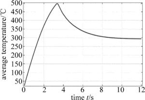
    Figure 4.  Relationship between average temperature and irradiation time

  • 图 5为CCD在激光辐照时刻t=3.4s时的应力及应变分布图。由图可知,在CCD的多层材料中,遮光Al膜层和基底Si层所受应力较大。图最大应力出现在基底Si下表面边缘处,由于是固定边界与自由边界的交汇处,受到CCD因温升而发生向上和向外的热膨胀所引起的应力同时作用。最小应力出现在SiO2增厚层的边缘。因此,判断CCD热应力破坏的位置应着重考虑基底Si下表面边缘处。

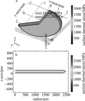
    Figure 5.  Material stress distribution at t=3.4s

    图 6a图 6b分别表示材料内部最大的应力及材料交界面的应力随时间的变化。由图可知,CCD中各材料受到的最大应力均为压应力,主要是受热膨胀所致。其中以Si下表面边缘处所受应力最大,峰值达到4140MPa,可是Si的抗压强度有限,为120MPa[3],也就是说当激光作用0.1s左右时,基底Si固定边缘就出现了滑移,随着辐照时间增加,滑移位置向中心移动。由图 6b可知,材料交界面处以遮光Al膜与上下层的SiO2膜层间的拉应力为最大。由于Al膜和SiO2的附着力为100MPa左右[12],所以当激光作用0.3s时,由光斑中心开始,遮光Al膜和SiO2膜层发生分离,并向边缘扩散。

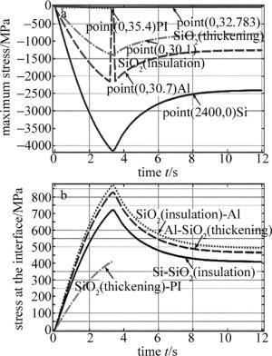
    Figure 6.  Relationship between thermal stress and irradiation time

  • 经以上分析,激光辐照首先使基底Si在固定底面边缘产生沿径向由外向内的滑移,紧接着遮光Al膜与SiO2膜层沿径向由内向外脱离,两种应力破坏可能伴随发生。遮光Al膜的脱离致使产生漏光现象,并且减少基底Si的向上热传导,减小了热量损失,加快了基底Si与固定底面的滑移分离。当基底Si完全脱落,离开光学系统的像面,整个系统将失效。

3.   结论
  • 激光对CCD的破坏主要是对其组成材料的熔融破坏和应力破坏。由分析可知,功率为0.5W的1.06μm连续激光以光斑半径1mm对CCD进行照射,在热破坏方面,微透镜PI将在激光辐照3.4s时, 首先达到阈值发生热分解作用,并且这种分解会使激光作用位置发生变化,加之存在热辐射和热对流等能量损失,各主要材料温度达不到熔点而不受熔融破坏;在应力破坏方面,基底Si因压应力达到材料强度,在激光辐照0.1s时, 开始在固定底面的边缘产生由外向内的滑移。随后,金属Al膜因交界面应力达到附着力的量级而发生脱离。由于应力破坏发生在热破坏之前,而且Al膜的脱离可能使热破坏终止,甚至不发生,但是对应力破坏起到加速作用。因此,应力破坏成为该型激光对CCD损伤的原因。最终,CCD会因整个器件脱离固定位置而导致系统失效。

Reference (18)

Catalog

    /

    DownLoad:  Full-Size Img  PowerPoint
    Return
    Return